
特長
- Multiplication of Input Frequency by 2, 3, 4, and 6
- Distribution of Output Frequency to 21 Outputs Organized in Three Output Banks: QA0-QA6, QB0-QB6, QC0-QC6, Each Fully Selectable
- Fully Integrated PLL
- Selectable Output Frequency Range Is 50 to 100 MHz and 100 to 200 MHz
- Selectable Input Frequency Range Is 16.67 to 33 MHz and 25 to 50 MHz
- LVCMOS Outputs
- Outputs Disable to High Impedance (Except QFB)
- LVCMOS or LVPECL Reference Clock Options
- 48-Lead QFP Packaging
- 48-Lead Pb-Free Package Available
- ± 50 ps Cycle-to-Cycle Jitter
- 150 ps Maximum Output-to-Output Skew
- 200 ps Maximum Static Phase Offset Window
説明
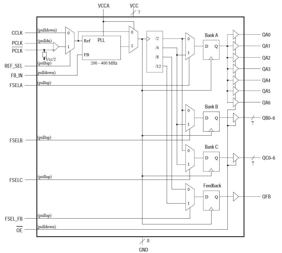
The MPC9600 is a fully LVCMOS 2.5 V or 3.3 V compatible PLL clock driver. The MPC9600 has the capability to generate clock signals of 50 to 200 MHz from clock sources of 16.67 to 50 MHz. The internal PLL is optimized for this frequency range and does not require external loop filter components. QFB provides an output for the external feedback path to the feedback input FB_IN. The QFB divider ratio is configurable and determines the PLL frequency multiplication factor when QFB is directly connected to FB_IN. The MPC9600 is optimized for minimizing the propagation delay between the clock input and FB_IN. Three output banks of 7 outputs each bank can be individually configured to divide the VCO frequency by 2 or by 4. Combining the feedback and output divider ratios, the MPC9600 is capable to multiply the input frequency by 2, 3, 4, and 6. The reference clock is selectable either LVPECL or LVCMOS. The LVPECL reference clock feature allows the designer to use LVPECL fanout buffers for the inner branches of the clock distribution tree. All control inputs accept LVCMOS compatible levels. The outputs provide low impedance LVCMOS outputs capable of driving parallel terminated 50 ? transmission to VTT= VCC/2. For series terminated lines the MPC9600 can drive two lines per output giving the device an effective total fanout of 1:42. With guaranteed maximum output-to-output skew of 150 ps, the MPC9600 PLL clock driver meets the synchronization requirements of the most demanding systems. The VCCA analog power pin doubles as a PLL bypass select line for test purpose. When the VCCA is driven to GND the reference clock will bypass the PLL. The device is packaged in a 48-lead LQFP package to provide optimum combination of board density and performance.