
特長
- 1.8 V CMOS compatible static digital inputs
- 1.8 V CMOS digital outputs
- 8-bit resolution
- Binary or 2's complement CMOS outputs
- Differential analog input
- High-speed sampling rate up to 250 MHz
- HTQFP48 package
- Industrial temperature range from -40°C to +85°C
- Integrated voltage regulator for input common-mode reference
- Integrated voltage regulator or external control for analog input full-scale
- Maximum analog input frequency up to 560 MHz
- Only 2 clock cycles latency
- Programmable acquisition output clock (complete conversion signal)
- Selectable 1.8 V CMOS or LVDS clock input
説明
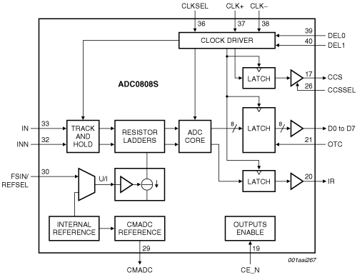
The ADC0808S is a differential, high-speed, 8-bit Analog-to-Digital Converter (ADC) optimized for telecommunication transmission control systems and tape drive applications. It allows signal sampling frequencies up to 250 MHz. The ADC0808S clock inputs are selectable between 1.8 V Complementary Metal Oxide Semiconductor (CMOS) or Low-Voltage Differential Signals (LVDS). The data output signal levels are 1.8 V CMOS. All static digital inputs (CLKSEL, CCSSEL, CE_N, OTC, DEL0 and DEL1) are 1.8 V CMOS compatible. The ADC0808S offers the most flexible acquisition control system possible due to its programmable Complete Conversion Signal (CCS) which allows the delay time of the acquisition clock and acquisition clock frequency to be adjusted. The ADC0808S is supplied in an HTQFP48 package.