
特長
- Eight 1MHz – 48MHz 1.05V LVCMOS outputs
- Additive cycle-to-cycle jitter < 8ps
- Output-to-output skew within a bank < 50ps
- Output-to-output skew between banks < 100ps
- 1.8V power supply, 15mW typical power consumption
- Three OE pins
- 1.05V LVCMOS inputs with VREF pin
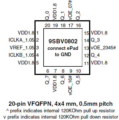
- Space saving 4mm x 4mm 20-VFQFPN
説明
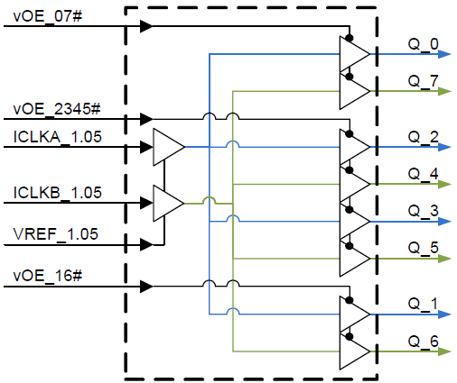
The 9SBV0802 provides two banks of four 1.05V LVCMOS outputs. Each bank has its own input. There are three OE pins. Two OE pins control two outputs each and one OE pin controls four outputs. One 9SBV0802 allows one PCH to easily support four CPUs with point-to-point routing of the PM signals. Two 9SBV0802 devices allow one PCH to easily support up to eight CPUs with point-to-point routing of the PM signals.
パラメータ
| 属性 | 値 |
|---|---|
| Temp. Range (°C) | -40 to 85°C |
| Product Category | Clock Buffers & Drivers |
パッケージオプション
| Pkg. Type | Pkg. Dimensions (mm) | Lead Count (#) | Pitch (mm) |
|---|---|---|---|
| VFQFPN | 4.0 x 4.0 x 1.0 | 20 | 0.5 |
アプリケーション
- Fanout buffer for PM-SYNC and PM_SYNC CLK in Intel servers