
特長
- PCIe Gen1–4 compliant
- LP-HCSL outputs; save 12 resistors compared to standard PCIe devices
- 54 mW typical power consumption; reduced thermal concerns
- Outputs can optionally be supplied from any voltage between 1.05 and 1.8 V; maximum power savings
- OE# pins; support DIF power management
- Programmable slew rate for each output; allows tuning for various line lengths
- Programmable output amplitude; allows tuning for various application environments
- DIF outputs blocked until PLL is locked; clean system start-up
- Selectable 0%, -0.25% or -0.5% spread on DIF outputs; reduces EMI
- External 25 MHz crystal; supports tight ppm with 0 ppm synthesis error
- Configuration can be accomplished with strapping pins; SMBus interface not required for device control
- 3.3 V tolerant SMBus interface works with legacy controllers
- Space saving 5x5 mm 40-pin VFQFPN; minimal board space
- Selectable SMBus addresses; multiple devices can easily share an SMBus segment

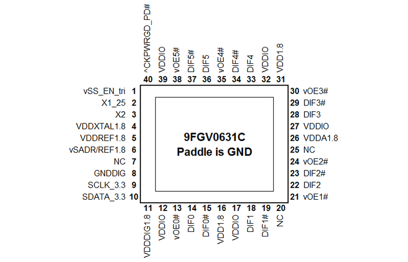
説明
The 9FGV0631 is a member of IDT's SOC-Friendly 1.8 V Very-Low-Power PCIe clock family. The device has 6 output enables for clock management, 2 different spread spectrum levels in addition to spread off and 2 selectable SMBus addresses.
| Part Number | Status | Samples | Stock | Package | Lead Count (#) | Carrier Type | Moisture Sensitivity Level (MSL) | Qty. per Reel (#) | Qty. per Carrier (#) | Pb (Lead) Free | Pb Free Category | Temp. Range (°C) |
|---|---|---|---|---|---|---|---|---|---|---|---|---|
| 9FGV0631CKILF | Obsolete | N/A | Out of Stock | VFQFPN | 40# | Tray | 3 | 0 | 490# | Yes | e3 Sn | -40 to 85°C |
| 9FGV0631CKILFT | Obsolete | N/A | Out of Stock | VFQFPN | 40# | Reel | 3 | 2500# | 0 | Yes | e3 Sn | -40 to 85°C |
| 9FGV0631CKLF | Obsolete | N/A | Out of Stock | VFQFPN | 40# | Tray | 3 | 0 | 490# | Yes | e3 Sn | 0 to 70°C |
| 9FGV0631CKLFT | Obsolete | N/A | In Stock | VFQFPN | 40# | Reel | 3 | 2500# | 0 | Yes | e3 Sn | 0 to 70°C |
- アプリケーションノート英語PDF 431 KB 7WDXRDKU4E7E-5-59216 2023年12月06日
- アプリケーションノート英語PDF 307 KB 7WDXRDKU4E7E-5-59989 2016年3月10日
- アプリケーションノート英語PDF 1.9 MB 7WDXRDKU4E7E-5-57315 2014年5月13日
- アプリケーションノート英語PDF 495 KB 7WDXRDKU4E7E-5-57312 2014年5月12日
- アプリケーションノート英語PDF 442 KB 7WDXRDKU4E7E-5-57298 2014年5月08日
- アプリケーションノート英語PDF 120 KB 7WDXRDKU4E7E-5-57289 2014年5月06日
- アプリケーションノート英語PDF 160 KB 7WDXRDKU4E7E-5-57287 2014年5月06日
推奨ドキュメント (1)
データシート (1)
No Results Found.
入力するワードを減らしてみたり、異なるワード、あるいはより一般的なワードを入力してみましょう。
フィルターを適用している場合、フィルターの範囲を見直してみてより広く検索結果が反映される様にしてみましょう。
- ナレッジベースを検索してみましょう。FAQにより、お客様をサポートいたします。
- ルネサスの技術スタッフやコミュニティからのヘルプをサポートフォーラムから受けられます。
- アプリケーションノート英語PDF 431 KB 7WDXRDKU4E7E-5-59216 2023年12月06日
- アプリケーションノート英語PDF 1.99 MB 7WDXRDKU4E7E-5-57242 2022年3月01日
- アプリケーションノート英語PDF 307 KB 7WDXRDKU4E7E-5-59989 2016年3月10日もっと見る (14)
アプリケーションノート、ホワイトペーパー (14)
製品通知(PCN、EOLなど) (6)
No Results Found.
入力するワードを減らしてみたり、異なるワード、あるいはより一般的なワードを入力してみましょう。
フィルターを適用している場合、フィルターの範囲を見直してみてより広く検索結果が反映される様にしてみましょう。
- ナレッジベースを検索してみましょう。FAQにより、お客様をサポートいたします。
- ルネサスの技術スタッフやコミュニティからのヘルプをサポートフォーラムから受けられます。
No Results Found.
入力するワードを減らしてみたり、異なるワード、あるいはより一般的なワードを入力してみましょう。
フィルターを適用している場合、フィルターの範囲を見直してみてより広く検索結果が反映される様にしてみましょう。
- ナレッジベースを検索してみましょう。FAQにより、お客様をサポートいたします。
- ルネサスの技術スタッフやコミュニティからのヘルプをサポートフォーラムから受けられます。
No Results Found.
入力するワードを減らしてみたり、異なるワード、あるいはより一般的なワードを入力してみましょう。
フィルターを適用している場合、フィルターの範囲を見直してみてより広く検索結果が反映される様にしてみましょう。
- ナレッジベースを検索してみましょう。FAQにより、お客様をサポートいたします。
- ルネサスの技術スタッフやコミュニティからのヘルプをサポートフォーラムから受けられます。
No Results Found.
入力するワードを減らしてみたり、異なるワード、あるいはより一般的なワードを入力してみましょう。
フィルターを適用している場合、フィルターの範囲を見直してみてより広く検索結果が反映される様にしてみましょう。
- ナレッジベースを検索してみましょう。FAQにより、お客様をサポートいたします。
- ルネサスの技術スタッフやコミュニティからのヘルプをサポートフォーラムから受けられます。
No Results Found.
入力するワードを減らしてみたり、異なるワード、あるいはより一般的なワードを入力してみましょう。
フィルターを適用している場合、フィルターの範囲を見直してみてより広く検索結果が反映される様にしてみましょう。
- ナレッジベースを検索してみましょう。FAQにより、お客様をサポートいたします。
- ルネサスの技術スタッフやコミュニティからのヘルプをサポートフォーラムから受けられます。
No Results Found.
入力するワードを減らしてみたり、異なるワード、あるいはより一般的なワードを入力してみましょう。
フィルターを適用している場合、フィルターの範囲を見直してみてより広く検索結果が反映される様にしてみましょう。
- ナレッジベースを検索してみましょう。FAQにより、お客様をサポートいたします。
- ルネサスの技術スタッフやコミュニティからのヘルプをサポートフォーラムから受けられます。
マーケティング資料 (1)
No Results Found.
入力するワードを減らしてみたり、異なるワード、あるいはより一般的なワードを入力してみましょう。
フィルターを適用している場合、フィルターの範囲を見直してみてより広く検索結果が反映される様にしてみましょう。
- ナレッジベースを検索してみましょう。FAQにより、お客様をサポートいたします。
- ルネサスの技術スタッフやコミュニティからのヘルプをサポートフォーラムから受けられます。
No Results Found.
入力するワードを減らしてみたり、異なるワード、あるいはより一般的なワードを入力してみましょう。
フィルターを適用している場合、フィルターの範囲を見直してみてより広く検索結果が反映される様にしてみましょう。
- ナレッジベースを検索してみましょう。FAQにより、お客様をサポートいたします。
- ルネサスの技術スタッフやコミュニティからのヘルプをサポートフォーラムから受けられます。
フィルター
適用されたフィルター
ソフトウェア/ツール
タイプでの検索
プロバイダでの検索
サンプルコード
アプリケーションでの検索
ファンクションでの検索
コンパイラでの検索
IDE に関するフィルタリング
シミュレーションモデル
Partner Solutions
No Results Found.
入力するワードを減らしてみたり、異なるワード、あるいはより一般的なワードを入力してみましょう。
フィルターを適用している場合、フィルターの範囲を見直してみてより広く検索結果が反映される様にしてみましょう。
- ナレッジベースを検索してみましょう。FAQにより、お客様をサポートいたします。
- ルネサスの技術スタッフやコミュニティからのヘルプをサポートフォーラムから受けられます。
No Results Found.
入力するワードを減らしてみたり、異なるワード、あるいはより一般的なワードを入力してみましょう。
フィルターを適用している場合、フィルターの範囲を見直してみてより広く検索結果が反映される様にしてみましょう。
- ナレッジベースを検索してみましょう。FAQにより、お客様をサポートいたします。
- ルネサスの技術スタッフやコミュニティからのヘルプをサポートフォーラムから受けられます。
No Results Found.
入力するワードを減らしてみたり、異なるワード、あるいはより一般的なワードを入力してみましょう。
フィルターを適用している場合、フィルターの範囲を見直してみてより広く検索結果が反映される様にしてみましょう。
- ナレッジベースを検索してみましょう。FAQにより、お客様をサポートいたします。
- ルネサスの技術スタッフやコミュニティからのヘルプをサポートフォーラムから受けられます。
シミュレーションモデル (1)
No Results Found.
入力するワードを減らしてみたり、異なるワード、あるいはより一般的なワードを入力してみましょう。
フィルターを適用している場合、フィルターの範囲を見直してみてより広く検索結果が反映される様にしてみましょう。
- ナレッジベースを検索してみましょう。FAQにより、お客様をサポートいたします。
- ルネサスの技術スタッフやコミュニティからのヘルプをサポートフォーラムから受けられます。
Ron Wade, chief PCIe system architect explains the fundamental difference in reference clock jitter budgets between the first three generations of the specification and those of Gen4 and Gen5 which raise new challenges for designers.
This whiteboard video presents a brief overview comparing the evolution of PCI Express data rates through five generations versus that of the common clock jitter specifications.
Renesas's chief PCIe system architect explains how to derive separate reference clock jitter limits from the PCI Express Gen4 and Gen5 specifications.
A detailed overview of IDT's full-featured PCI Express (PCIe) clock and timing solutions. The presentation addresses PCIe Gen 1, Gen 2, Gen 3, and Gen 4 architectures and how IDT's industry-leading solutions provide all the functions, features, and performance required by the application.
Presented by Ron Wade, System Architect at IDT. For more information visit the PCIe clocks page.
This is the first video in our PCIe series. In this video, we define PCIe architectures, focusing on common and separate clock architectures. Watch the rest of the video series below where Ron will cover the impact of different timing architectures.
In this episode, Ron Wade from IDT (acquired by Renesas) explains PCIe common clocking and its impact on timing solutions. Learn about using a single clock source, fan-out buffers, and the considerations for spread spectrum and non-spread spectrum clocking in PCIe systems.
In this video, we explore PCIe with separate reference clocks and the effects of clock selection. Learn how separate reference clocks work and their impact on system performance and stability.
This video provides a high-level overview of Separate Reference Clock with Independent Spread (SRIS) architectures for PCI Express systems, additional performance requirements that this clocking architecture imposes on the reference clocks, and some system implications encountered trying to implement the architecture.
IDT (acquired by Renesas) engineer provides a brief tutorial describing the main differences between standard HCSL and low-power HCSL (LP-HCSL).
Presented by Ron Wade, PCI Express timing expert.
An overview of IDT's full-featured PCI Express (PCIe) clock generators addressing PCIe Gen 1, Gen 2, Gen 3, and Gen 4.
Presented by Ron Wade, System Architect at IDT.
An overview of PCI Express applications and how IDT's industry-leading portfolio of PCIe clock products addresses the requirements. The video briefly discusses PCIe riser cards, embedded SOC, and PCIe storage (NVME) examples.
Presented by Ron Wade, System Architect at IDT.
A brief overview of how data rates have changed from PCI Express (PCIe) Generation 1, Gen 2, Gen 3, Gen 4 and Gen 5.
Presented by Ron Wade, system architect at IDT.
A brief overview of how clock and timing specifications have changed from PCI Express (PCIe) Generation 1, Gen 2, Gen 3, Gen 4 and Gen 5.
Presented by Ron Wade, system architect at IDT (acquired by Renesas).
A brief overview of the PCI Express common clock (CC) jitter model, and the transfer functions as they relate to the timing PLLs. This model applies to PCI Express (PCIe) Gen 2, Gen 3, Gen 4 and Gen 5. The equations would be slightly different for other PCIe architectures, such as SRIS, SRnS, or data clocked.
Presented by Ron Wade, system architect at IDT (acquired by Renesas). For more information about Renesas's PCIe timing solutions, visit the PCI Express (PCIe) Clocks page.


