パッケージ情報
| CADモデル: | View CAD Model |
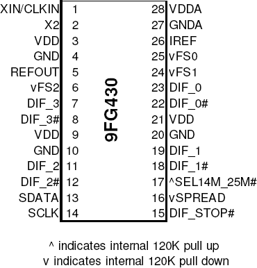
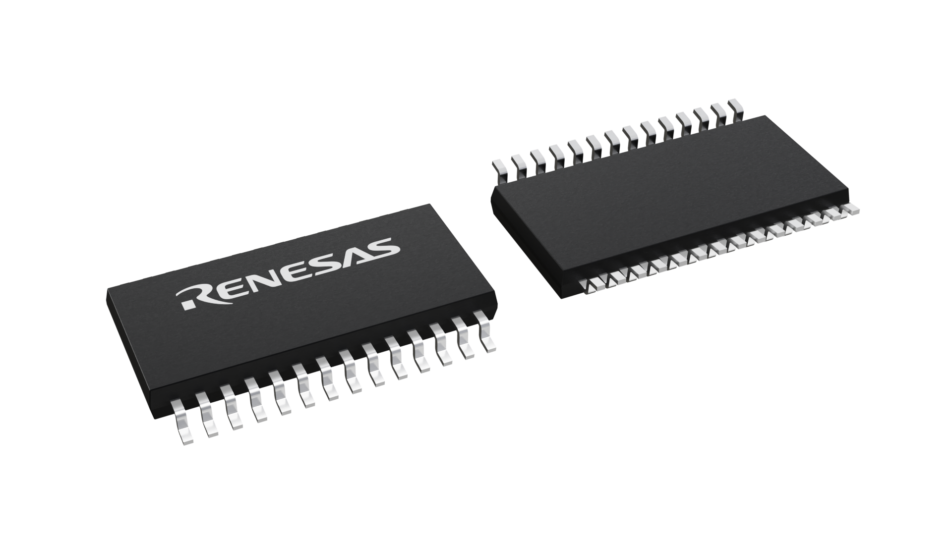
| Pkg. Type: | TSSOP |
| Pkg. Code: | PGG28 |
| Lead Count (#): | 28 |
| Pkg. Dimensions (mm): | 9.7 x 4.4 x 1.0 |
| Pitch (mm): | 0.65 |
環境及び輸出分類情報
| Moisture Sensitivity Level (MSL) | 1 |
| Pb (Lead) Free | Yes |
| ECCN (US) | EAR99 |
| HTS (US) | 8542.39.0090 |
製品スペック
| Lead Count (#) | 28 |
| Carrier Type | Reel |
| Moisture Sensitivity Level (MSL) | 1 |
| Qty. per Reel (#) | 2000 |
| Qty. per Carrier (#) | 0 |
| Package Area (mm²) | 42.7 |
| Pkg. Dimensions (mm) | 9.7 x 4.4 x 1.0 |
| Pb (Lead) Free | Yes |
| Pb Free Category | e3 Sn |
| Temp. Range (°C) | -40 to 85°C |
| Advanced Features | Programmable Clock, Spread Spectrum, Reference Output |
| App Jitter Compliance | PCIe Gen1, PCIe Gen2, PCIe Gen3 |
| Architecture | Common |
| C-C Jitter Max P-P (ps) | 50 |
| Core Voltage (V) | 3.3 |
| Diff. Output Signaling | HCSL |
| Diff. Outputs | 4 |
| Diff. Termination Resistors | 16 |
| Input Freq (MHz) | 14.3182 - 14.3182, 25 - 25 |
| Input Type | Crystal, LVCMOS |
| Inputs (#) | 1 |
| Length (mm) | 9.7 |
| MOQ | 2000 |
| Output Freq Range (MHz) | 100 - 100, 125 - 125, 133.33 - 133.33, 166.67 - 166.67, 200 - 200, 266.67 - 266.67, 333.33 - 333.33, 400 - 400 |
| Output Skew (ps) | 50 |
| Output Type | HCSL, LVCMOS |
| Output Voltage (V) | 0.8V, 3.3V |
| Outputs (#) | 5 |
| PLL | Yes |
| Phase Jitter Max RMS (ps) | 0.2 |
| Pitch (mm) | 0.65 |
| Pkg. Type | TSSOP |
| Power Consumption Typ (mW) | 347 |
| Prog. Clock | No |
| Prog. Interface | SMBUS |
| Reel Size (in) | 13 |
| Reference Output | Yes |
| Requires Terms and Conditions | Does not require acceptance of Terms and Conditions |
| Spread Spectrum | Yes |
| Supply Voltage (V) | 3.3 - 3.3 |
| Tape & Reel | Yes |
| Thickness (mm) | 1 |
| Width (mm) | 4.4 |
| Xtal Freq (MHz) | 14.318 - 14.318, 25 - 25 |
| Xtal Inputs (#) | 1 |
| 掲載 | No |
9FG430 に関するリソース
説明
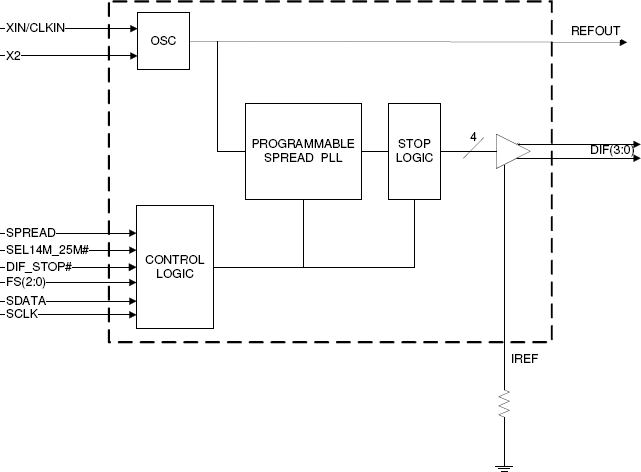
The 9FG430 is a Frequency Timing Generator that provides 4 HCSL differential output pairs. These outputs support PCI-Express Gen3, and QPI applications. The part supports Spread Spectrum and synthesizes several additional output frequencies from either a 14.31818 MHz crystal, a 25 MHz crystal or reference input clock. The 9FG430 also outputs a copy of the reference clock. Complete control of the device is available via strapping pins or via the SMBus interface.


