
特長
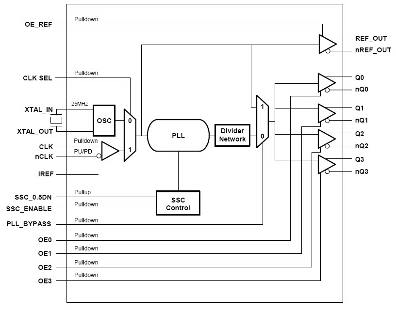
- Four 0.7V current mode differential HCSL output pairs
- One 0.7V current mode differential HCSL reference output
- CLK, nCLK input can accept the following input levels: HCSL, LVDS, LVPECL, LVHSTL
- Crystal oscillator interface: 25MHz
- Output frequency: 100MHz
- RMS phase jitter @ 100MHz (12kHz – 20MHz): 1.2ps (typical)
- Spread Spectrum for electromagnetic interference (EMI) reduction
- Individual output control via output enable pins
- In bypass mode functions as a 1 to 5 fanout buffer
- PCI Express® (2.5 Gb/S), Gen 2 (5 Gb/s) and Gen 3 (8 Gb/s) jitter compliant
- 3.3V operating supply mode
- -40°C to 85°C ambient operating temperature
- Available lead-free (RoHS 6) package
説明
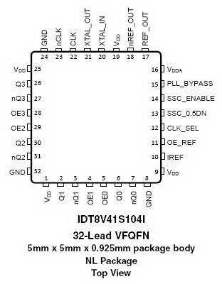
The 8V41S104I is a PLL-based clock generator specifically designed for PCI Express® Generation 3 applications. This device generates a 100MHz differential HCSL clock from an input reference of 25MHz. The input reference may be derived from an external source or by the addition of a 25MHz crystal to the on-chip crystal oscillator. The device offers spread spectrum clock output for reduced EMI applications. The spread spectrum control pins are used to enable or disable spread spectrum operation, as well as selecting either a down spread value of -0.35% or -0.5%. The enable and disable for each of the outputs is controlled via individual output enable pins. The 8V41S104I is packaged in a compact, lead-free (RoHS 6) 32-lead VFQFN package. The industrial temperature range supports high-end computing, telecommunication, and networking end equipment requirements.