
特長
- Three output banks, consisting of eight LVDS output pairs total
- INx, nINx inputs can accept the following differential input levels: LVPECL, LVDS, CML
- Selectable output divider values of ÷1, ÷2, and ÷4
- Maximum output frequency: 1.5GHz
- Maximum input frequency: 3GHz
- Bank Skew: 10ps (typical)
- Part-to-part skew: 100ps (typical)
- Additive phase jitter, RMS: 0.170ps (typical)
- Propagation delay: 802ps (typical)
- Output rise time: 150ps (typical)
- 2.5V ±5% operating supply voltage
- -40 °C to 85 °C ambient operating temperature
- Available in lead-free (RoHS 6) package
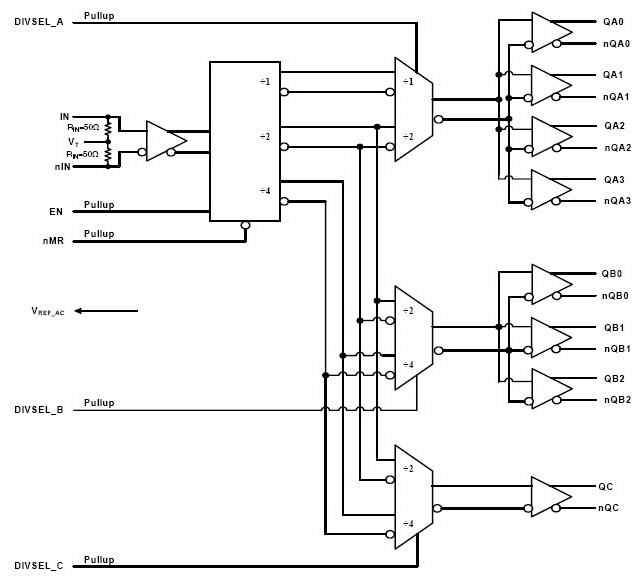
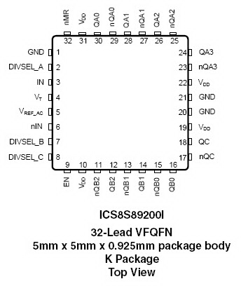
8S89200I - Block Diagram
説明
The 8S89200I is a high-speed 1-to-8 differential-to-LVDS clock divider that is optimized for high speed and very low output skew, making it suitable for use in demanding applications such as SONET, 1 Gigabit and 10 Gigabit Ethernet, and Fibre Channel. The internally terminated differential inputs and VREF_AC pins allow other differential signal families such as LVPECL, LVDS, and CML to be easily interfaced to the input with minimal use of external components.
The device also has a selectable ÷1, ÷2, ÷4 output divider, which can allow the part to support multiple output frequencies from the same reference clock. The 8S89200I is packaged in a small 5mm x 5mm 32-pin VFQFN package which makes it ideal for use in space-constrained applications.


