
| CADモデル: | View CAD Model |
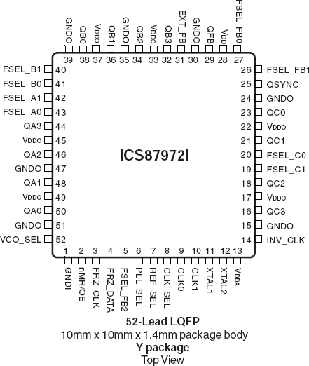
| Pkg. Type: | TQFP |
| Pkg. Code: | PPG52 |
| Lead Count (#): | 52 |
| Pkg. Dimensions (mm): | 10.0 x 10.0 x 1.4 |
| Pitch (mm): | 0.65 |
| Moisture Sensitivity Level (MSL) | 3 |
| Pb (Lead) Free | Yes |
| ECCN (US) | EAR99 |
| HTS (US) | 8542.39.0090 |
| Lead Count (#) | 52 |
| Carrier Type | Tray |
| Moisture Sensitivity Level (MSL) | 3 |
| Qty. per Reel (#) | 0 |
| Qty. per Carrier (#) | 160 |
| Pb (Lead) Free | Yes |
| Pb Free Category | e3 Sn |
| Temp. Range (°C) | -40 to 85°C |
| Advanced Features | Programmable Clock, Feedback Input |
| C-C Jitter Typ P-P (ps) | 100 |
| Core Voltage (V) | 3.3 |
| Feedback Input | Yes |
| Input Freq (MHz) | 10 - 120 |
| Input Type | Crystal, LVCMOS |
| Inputs (#) | 3 |
| Length (mm) | 10 |
| MOQ | 160 |
| Output Banks (#) | 4 |
| Output Freq Range (MHz) | 8.33 - 125 |
| Output Skew (ps) | 550 |
| Output Type | LVCMOS |
| Output Voltage (V) | 3.3 |
| Outputs (#) | 13 |
| Package Area (mm²) | 100 |
| Pitch (mm) | 0.65 |
| Pkg. Dimensions (mm) | 10.0 x 10.0 x 1.4 |
| Pkg. Type | TQFP |
| Product Category | Zero Delay Buffers |
| Prog. Clock | Yes |
| Prog. Interface | Serial |
| Requires Terms and Conditions | Does not require acceptance of Terms and Conditions |
| Tape & Reel | No |
| Thickness (mm) | 1.4 |
| Width (mm) | 10 |
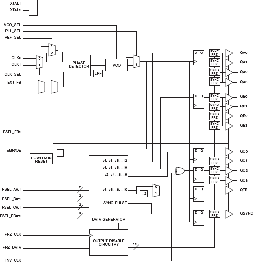
The 87972I is a low skew, LVCMOS/LVTTL Clock Generator. The 87972I has three selectable inputs and provides fourteen LVCMOS/LVTTL outputs. The 87972I is a highly flexible device. Using the crystal oscillator input, it can be used to generate clocks for a system. All of these clocks can be the same frequency or the device can be configured to generate up to three different frequencies among the three output banks. Using one of the single ended inputs, the 87972I can be used as a zero delay buffer/multiplier/divider in clock distribution applications. The three output banks and feedback output each have their own output dividers which allows the device to generate a multitude of different bank frequency ratios and output-to-input frequency ratios. In addition, 2 outputs in Bank C (QC2, QC3) can be selected to be inverting or non-inverting. The output frequency range is 8.33MHz to125MHz. Input frequency range is 5MHz to 120MHz. The 87972I also has a QSYNC output which can be used for system synchronization purposes. It monitors Bank A and Bank C outputs and goes low one period of the faster clock prior to coincident rising edges of Bank A and Bank C clocks. QSYNC then goes high again when the coincident rising edges of Bank A and Bank C occur. This feature is used primarily in applications where Bank A and Bank C are running at different frequencies, and is particularly useful when they are running at non-integer multiples of one another.