
特長
- Five differential LVDS outputs designed to meet or exceed the requirements of ANSI TIA/EIA-644
- Selectable differential clock inputs
- CLKx, nCLKx pairs can accept the following differential input levels: LVPECL, LVDS, LVHSTL, HCSL, SSTL
- Output frequency range: 31.25MHz to 700MHz
- Input frequency range: 31.25MHz to 700MHz
- VCO range: 250MHz to 700MHz
- External feedback for "zero delay" clock regeneration with configurable frequencies
- Programmable dividers allow for the following output-to-input frequency ratios: 8:1, 4:1, 2:1, 1:1, 1:2, 1:4, 1:8
- Cycle-to-cycle jitter: 30ps (maximum)
- Output skew: 40ps (maximum)
- Static phase offset: 25ps ± 125ps
- Full 3.3V supply voltage
- -40°C to 85°C ambient operating temperature
- Available in both standard (RoHS 5) and lead-free (RoHS 6) packages
説明
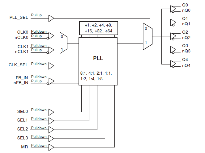
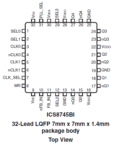
The 8745BI is a highly versatile 1:5 LVDS Clock Generator and a member of the HiPerClockS™ family of High Performance Clock Solutions from IDT. The 8745BI has a fully integrated PLL and can be configured as zero delay buffer, multiplier or divider, and has an output frequency range of 31.25MHz to 700MHz. The Reference Divider, Feedback Divider and Output Divider are each programmable, thereby allowing for the following output-to-input frequency ratios: 8:1, 4:1, 2:1, 1:1, 1:2, 1:4, 1:8. The external feedback allows the device to achieve "zero delay" between the input clock and the output clocks. The PLL_SEL pin can be used to bypass the PLL for system test and debug purposes. In bypass mode, the reference clock is routed around the PLL and into the internal output dividers.