
特長
- Ten differential 3.3V LVPECL outputs
- Selectable differential CLK0, nCLK0 or LVCMOS/LVTTL CLK1 inputs
- CLK0, nCLK0 supports the following input types: LVPECL, LVDS, LVHSTL, SSTL, HCSL
- CLK1 accepts the following input levels: LVCMOS or LVTTL
- Maximum output frequency: 350MHz
- VCO range: 250MHz to 700MHz
- External feedback for "zero delay" clock regeneration with configurable frequencies
- Cycle-to-cycle jitter: CLK0, nCLK0, 50ps (maximum) CLK1, 80ps (maximum)
- Output skew: 150ps (maximum)
- Static phase offset: -150ps to 150ps
- Lead-Free package fully RoHS compliant
説明
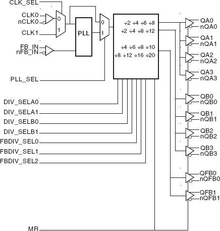
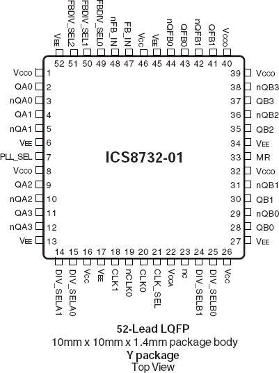
The 8732-01 is a low voltage, low skew, 3.3V LVPECL Clock Generator. The 8732-01 has two selectable clock inputs. The CLK0, nCLK0 pair can accept most standard differential input levels. The single ended clock input accepts LVCMOS or LVTTL input levels. The 8732-01 has a fully integrated PLL along with frequency configurable outputs. An external feedbackinput and outputs regenerate clocks with "zero delay". The 8732-01 has multiple divide select pins for each bank of outputs along with 3 independent feedback divide select pins allowing the 8732-01 to function both as a frequency multiplier and divider. The PLL_SEL input can be usedto bypass the PLL for test and system debug purposes.In bypass mode, the input clock is routed around the PLLand into the internal output dividers.


