

| CADモデル: | View CAD Model |
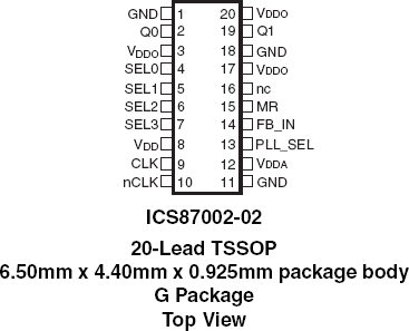
| Pkg. Type: | TSSOP |
| Pkg. Code: | PGG20 |
| Lead Count (#): | 20 |
| Pkg. Dimensions (mm): | 6.5 x 4.4 x 1.0 |
| Pitch (mm): | 0.65 |
| Moisture Sensitivity Level (MSL) | 1 |
| Pb (Lead) Free | Yes |
| ECCN (US) | EAR99 |
| HTS (US) | 8542.39.0090 |
| Lead Count (#) | 20 |
| Carrier Type | Reel |
| Moisture Sensitivity Level (MSL) | 1 |
| Qty. per Reel (#) | 3000 |
| Qty. per Carrier (#) | 0 |
| Pb (Lead) Free | Yes |
| Pb Free Category | e3 Sn |
| Temp. Range (°C) | 0 to 70°C |
| Advanced Features | Feedback Input |
| C-C Jitter Max P-P (ps) | 45 |
| Core Voltage (V) | 2.5V, 3.3V |
| Feedback Input | Yes |
| Input Freq (MHz) | 15.625 - 250 |
| Input Type | HCSL, HSTL, LVDS, LVPECL, SSTL |
| Inputs (#) | 1 |
| Length (mm) | 6.5 |
| MOQ | 3000 |
| Output Banks (#) | 1 |
| Output Freq Range (MHz) | 15.625 - 250 |
| Output Skew (ps) | 35 |
| Output Type | LVCMOS |
| Output Voltage (V) | 2.5V, 3.3V |
| Outputs (#) | 2 |
| Package Area (mm²) | 28.6 |
| Pitch (mm) | 0.65 |
| Pkg. Dimensions (mm) | 6.5 x 4.4 x 1.0 |
| Pkg. Type | TSSOP |
| Product Category | Zero Delay Buffers |
| Prog. Clock | No |
| Reel Size (in) | 13 |
| Requires Terms and Conditions | Does not require acceptance of Terms and Conditions |
| Tape & Reel | Yes |
| Thickness (mm) | 1 |
| Width (mm) | 4.4 |
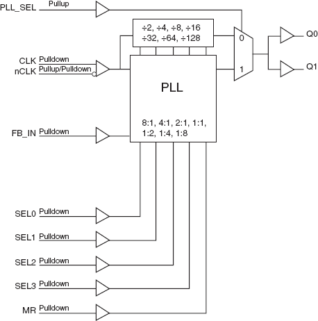
The 87002-02 is a highly versatile 1:2 Differential-to- LVCMOS/LVTTL Clock Generator. The 87002-02 has a differential clock input. The CLK, nCLK pair can accept most standard differential input levels. Internal bias on the nCLK input allows the CLK input to accept LVCMOS/LVTTL. The 87002-02 has a fully integrated PLL and can be configured as zero delay buffer, multiplier or divider and has an input and output frequency range of 15.625MHz to 250MHz. The reference divider, feedback divider and output divider are each programmable, thereby allowing for the following output-to-input frequency ratios: 8:1, 4:1, 2:1, 1:1, 1:2, 1:4, 1:8. The external feedback allows the device to achieve "zero delay" between the input clock and the output clocks. The PLL_SEL pin can be used to bypass the PLL for system test and debug purposes. In bypass mode, the reference clock is routed around the PLL and into the internal output dividers.