
| CADモデル: | View CAD Model |
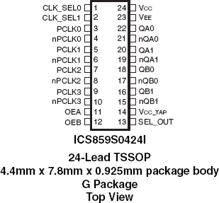
| Pkg. Type: | TSSOP |
| Pkg. Code: | PGG24 |
| Lead Count (#): | 24 |
| Pkg. Dimensions (mm): | 7.8 x 4.4 x 1.0 |
| Pitch (mm): | 0.65 |
| Moisture Sensitivity Level (MSL) | 1 |
| Pb (Lead) Free | Yes |
| ECCN (US) | EAR99 |
| HTS (US) | 8542.39.0090 |
| Lead Count (#) | 24 |
| Carrier Type | Tube |
| Moisture Sensitivity Level (MSL) | 1 |
| Qty. per Reel (#) | 0 |
| Qty. per Carrier (#) | 62 |
| Pb (Lead) Free | Yes |
| Pb Free Category | e3 Sn |
| Temp. Range (°C) | -40 to 85°C |
| Additive Phase Jitter Typ RMS (fs) | 220 |
| Additive Phase Jitter Typ RMS (ps) | 0.22 |
| Adjustable Phase | No |
| Advanced Features | Universal outputs |
| Channels (#) | 1 |
| Core Voltage (V) | 2.5V, 3.3V |
| Function | Buffer, Multiplexer |
| Input Freq (MHz) | 3000 |
| Input Type | CML, LVDS, LVPECL |
| Inputs (#) | 4 |
| Length (mm) | 7.8 |
| MOQ | 62 |
| Output Banks (#) | 1 |
| Output Freq Range (MHz) | 3000 |
| Output Skew (ps) | 25 |
| Output Type | LVDS, LVPECL |
| Output Voltage (V) | 2.5V, 3.3V |
| Outputs (#) | 4 |
| Package Area (mm²) | 34.3 |
| Pitch (mm) | 0.65 |
| Pkg. Dimensions (mm) | 7.8 x 4.4 x 1.0 |
| Pkg. Type | TSSOP |
| Product Category | Clock Buffers & Drivers, Clock Multiplexers, RF Buffers |
| Prog. Interface | Pin select |
| Requires Terms and Conditions | Does not require acceptance of Terms and Conditions |
| Supply Voltage (V) | 2.5 - 2.5, 3.3 - 3.3 |
| Tape & Reel | No |
| Thickness (mm) | 1 |
| Width (mm) | 4.4 |
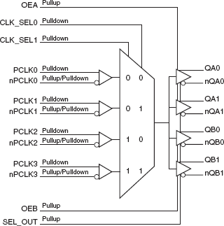
The 859S0424I is a 4:4 Differential-to-LVPECL/ LVDS Clock Multiplexer which can operate up to 3GHz. The outputs for this device can either be programmed to give LVPECL or LVDS levels. The 859S0424I has four selectable differential PCLKx, nPCLKx clock inputs. The PCLKx, nPCLKx input pairs can accept LVPECL, LVDS or CML levels. The fully differential architecture and low propagation delay make it ideal for use in clock distribution circuits.