
特長
- One LVDS level output
- One differential clock input pair
- Differential input clock (IN, nIN) can accept the following signaling levels: LVPECL, LVDS, CML
- Maximum frequency: 1.2GHz
- Programmable delay range: 2.2ns to 12.5ns in 10ps steps
- D[9:0] can accept LVPECL, LVCMOS, or LVTTL levels
- Full 3.3V supply voltages
- -40 °C to 85 °C ambient operating temperature
- Available in lead-free (RoHS 6) package
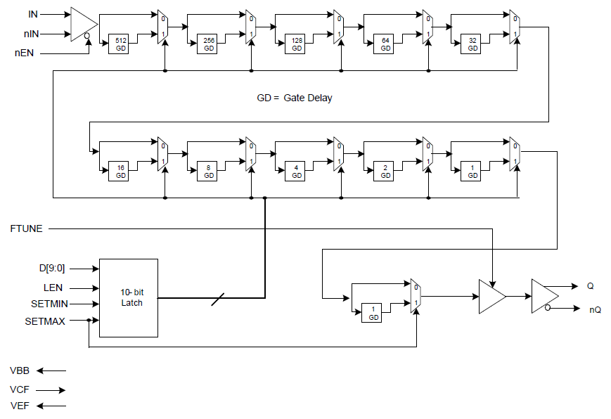

854S296I-33 - Block Diagram
説明
The ICS854S296I-33 is a high-performance LVDS programmable delay line. The delay can vary from 2.2ns to 12.5ns in 10ps steps. The ICS854S296I-33 is characterized to operate from a 3.3V power supply and is guaranteed over the industrial temperature range. The delay of the device varies in discrete steps based on a control word. A 10-bit long control word sets the delay in 10ps increments. Also, the input pins IN and nIN default to an equivalent low state when left floating. The control register can accept CMOS or TTL-level signals.


