
特長
- Ten differential LVPECL/ECL outputs
- Two selectable differential input pairs
- PCLK, nPCLK pair can accept the following differential input levels: LVPECL, LVDS, SSTL, CML
- CLK, nCLK pair can accept the following differential input levels: HSTL, LVPECL, LVDS, SSTL, HCSL
- Maximum input frequency: 2.7GHz
- Output skew: 35ps (maximum)
- Part-to-part skew: 250ps (maximum), fo > 1.5GHz
- Additive phase jitter, RMS: 0.123ps (typical)
- LVPECL and HSTL mode operating voltage supply range: VCC = 2.5V±5% or 3.3V±5%, VEE = 0V
- ECL mode operating voltage supply range: VEE = -3.3V±5% or -2.5V±5%, VCC = 0V
- -40°C to 85°C ambient operating temperature
- Available in lead-free (RoHS 6) package

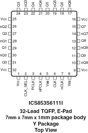
説明
The 853S6111I is a low skew 1-to-10 Differential Fanout Buffer, designed with clock distribution in mind, accepting two clock sources into an input MUX. The MUX is controlled by a CLK_SEL pin. This makes the 853S6111I very versatile, in that, it can operate as both a differential clock buffer as well as a signal-level translator and fanout buffer. The device is designed on a SiGe process and can operate up to frequencies of 2.7GHz. This ensures negligible jitter introduction to the timing budget which makes it an ideal choice for distributing high frequency, high precision clocks across back planes and boards in communication systems. Internal temperature compensation guarantees consistent performance across various platforms.