
| CADモデル: | View CAD Model |
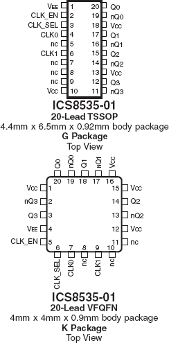
| Pkg. Type: | VFQFPN |
| Pkg. Code: | NLG20 |
| Lead Count (#): | 20 |
| Pkg. Dimensions (mm): | 4.0 x 4.0 x 1.0 |
| Pitch (mm): | 0.5 |
| Moisture Sensitivity Level (MSL) | 1 |
| Pb (Lead) Free | Yes |
| ECCN (US) | EAR99 |
| HTS (US) | 8542.39.0090 |
| Lead Count (#) | 20 |
| Carrier Type | Tray |
| Moisture Sensitivity Level (MSL) | 1 |
| Qty. per Reel (#) | 0 |
| Qty. per Carrier (#) | 490 |
| Package Area (mm²) | 16 |
| Pitch (mm) | 0.5 |
| Pkg. Dimensions (mm) | 4.0 x 4.0 x 1.0 |
| Pb (Lead) Free | Yes |
| Pb Free Category | e3 Sn |
| Temp. Range (°C) | 0 to 70°C |
| Additive Phase Jitter Typ RMS (fs) | 90 |
| Additive Phase Jitter Typ RMS (ps) | 0.09 |
| Core Voltage (V) | 3.3 |
| Function | Buffer, Multiplexer |
| Input Freq (MHz) | 266 |
| Input Type | LVCMOS |
| Inputs (#) | 2 |
| Length (mm) | 4 |
| MOQ | 2550 |
| Output Banks (#) | 1 |
| Output Freq Range (MHz) | 266 |
| Output Skew (ps) | 30 |
| Output Type | LVPECL |
| Output Voltage (V) | 3.3 |
| Outputs (#) | 4 |
| Pkg. Type | VFQFPN |
| Product Category | Clock Buffers & Drivers, Clock Multiplexers |
| Requires Terms and Conditions | Does not require acceptance of Terms and Conditions |
| Tape & Reel | No |
| Thickness (mm) | 1 |
| Width (mm) | 4 |
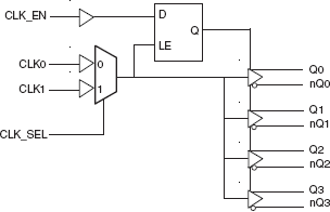
The 8535-01 is a low skew, high performance 1-to-4 LVCMOS/LVTTL-to-3.3V LVPECL fanout buffer and a member of the HiPerClockS™ family of High Performance Clock Solutions from IDT. The 8535-01 has two single ended clock inputs. the single ended clock input accepts LVCMOS or LVTTL input levels and translate them to 3.3V LVPECL levels. The clock enable is internally synchronized to eliminate runt clock pulses on the output during asynchronous assertion/deassertion of the clock enable pin. Guaranteed output and part-to-part skew characteristics make the 8535-01 ideal for those applications demanding well defined performance and repeatability.
