
| CADモデル: | View CAD Model |
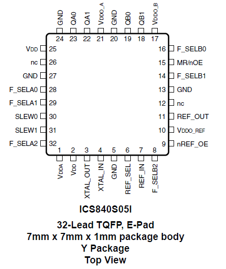
| Pkg. Type: | PTQFP |
| Pkg. Code: | DXG32 |
| Lead Count (#): | 32 |
| Pkg. Dimensions (mm): | 7.0 x 7.0 x 1.0 |
| Pitch (mm): | 0.8 |
| Moisture Sensitivity Level (MSL) | 3 |
| Pb (Lead) Free | Yes |
| ECCN (US) | EAR99 |
| HTS (US) | 8542.39.0090 |
| Lead Count (#) | 32 |
| Carrier Type | Tray |
| Moisture Sensitivity Level (MSL) | 3 |
| Pb (Lead) Free | Yes |
| Pb Free Category | e3 Sn |
| Temp. Range (°C) | -40 to 85°C |
| Core Voltage (V) | 3.3 |
| Divider Value | 12, 15, 16, 20, 24, 30, 40, 60 |
| Feedback Divider | 80 - 80 |
| Feedback Input | No |
| Input Freq (MHz) | 25 - 25 |
| Input Type | LVCMOS, Crystal |
| Inputs (#) | 2 |
| Length (mm) | 7 |
| MOQ | 250 |
| Output Banks (#) | 3 |
| Output Freq Range (MHz) | 33 - 200 |
| Output Signaling | LVCMOS |
| Output Skew (ps) | 40 |
| Output Type | LVCMOS |
| Output Voltage (V) | 3.3V, 2.5V |
| Outputs (#) | 5 |
| Package Area (mm²) | 49 |
| Period Jitter Typ P-P (ps) | 3.5 |
| Pitch (mm) | 0.8 |
| Pkg. Dimensions (mm) | 7.0 x 7.0 x 1.0 |
| Pkg. Type | PTQFP |
| Product Category | General Purpose Clocks |
| Prog. Clock | No |
| Qty. per Carrier (#) | 250 |
| Qty. per Reel (#) | 0 |
| Reference Output | Yes |
| Requires Terms and Conditions | Does not require acceptance of Terms and Conditions |
| Spread Spectrum | No |
| Tape & Reel | No |
| Thickness (mm) | 1 |
| Width (mm) | 7 |
| Xtal Freq (KHz) | 25 - 25 |
| Xtal Inputs (#) | 1 |
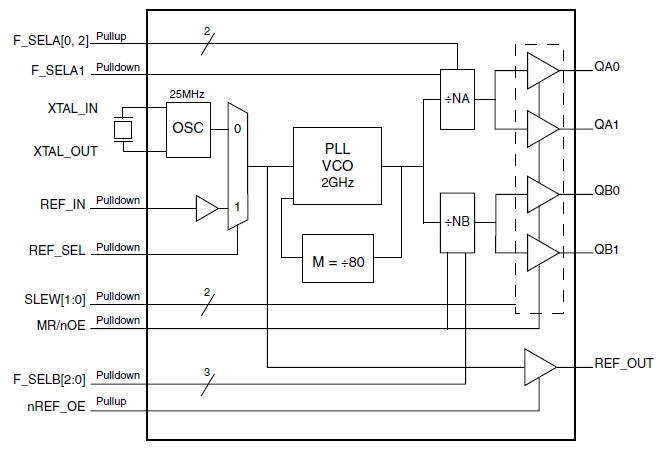
The 840S05I is a four output, Crystal or single ended-to-LVCMOS/LVTTL Frequency Synthesizer and a member of family of high performance clock solutions from IDT. The 840S05I uses a 25MHz parallel resonant crystal to generate 33.33MHz – 166.67MHz clock signals, replacing solutions requiring multiple oscillator and fan-out buffer solution. The device supports output slew rate control with two slew select pins (SLEW[1:0]). The VCO operates at a frequency of 2GHz. The device has 2 output banks, Bank A with two 33.33MHz – 166.67MHz LVCMOS/LVTTL outputs and Bank B with two 33.33MHz – 166.67MHz LVCMOS/LVTTL outputs.
The two banks have their own dedicated frequency select pins and can be independently set for the frequencies mentioned above. The low phase noise characteristic of the 840S05I makes it an ideal clock source for Gigabit Ethernet application. Designed for networking and industrial applications, the 840S05I can also drive the high-speed clock inputs of communication processors, DSPs, switches and bridges.