
特長
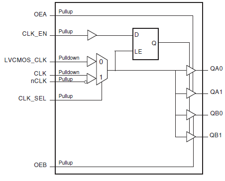
- Four LVCMOS/LVTTL outputs, (two banks of two LVCMOS outputs)
- Selectable differential CLK, nCLK pair or LVCMOS_CLK input
- CLK, nCLK pair can accept the following differential input levels: LVPECL, LVDS, LVHSTL, HCSL
- LVCMOS_CLK supports the following input types: LVCMOS, LVTTL
- Maximum output frequency: 250MHz
- Output skew: 100ps (maximum)
- Power supply modes:
- Core/Output
- 3.3V/3.3V
- 3.3V/2.5V
- 3.3V/1.8V
- 3.3V/1.5V
- -40 °C to 85 °C ambient operating temperature
- Lead-free (RoHS 6) packaging
説明
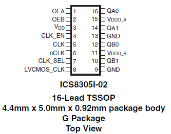
The 8305I-02 is a low skew, 1-to-4, differential/LVCMOS-to-LVCMOS/LVTTL fanout buffer. The 8305I-02 has selectable clock inputs that accept either differential or single-ended input levels. The clock enable is internally synchronized to eliminate runt pulses on the outputs during asynchronous assertion/de-assertion of the clock enable pin. Outputs are forced low when the clock is disabled. A separate output enable pin controls whether the outputs are in the active or high impedance state. Guaranteed output and part-to-part skew characteristics make the 8305I-02 ideal for those applications demanding well-defined performance and repeatability.