
特長
- Packaged in 16 pin SOIC (Pb-free, ROHS compliant)
- Access to VCO input and feedback paths of PLL
- VCO operating range up to 120 MHz (5V)
- Able to lock MHz range outputs to kHz range inputs through the use of external dividers
- Output Enable tri-states outputs
- Low skew output clocks
- Power Down turns off chip
- VCO predivide to feedback divider of 1 or 4
- 25 mA output drive capability at TTL levels
- Advanced, low power, sub-micron CMOS process
- Single supply +3.3 V or +5 V ±10% operating voltage
- Industrial temperature range available
- Forms a complete PLL, using the 674-01
- For better jitter performance, please use the MK1575
説明
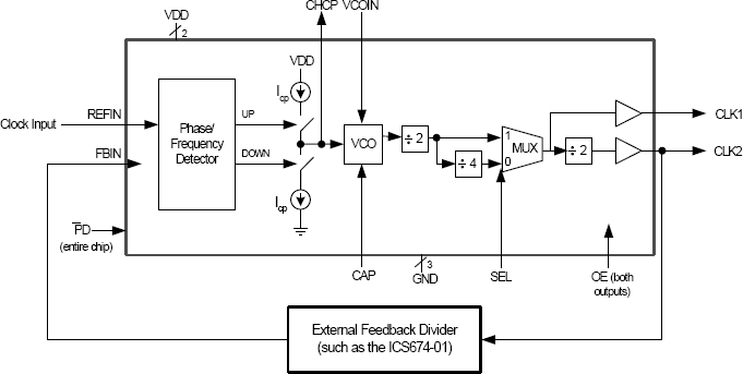
The 673-01 is a low cost, high performance Phase Locked Loop (PLL) designed for clock synthesis and synchronization. Included on the chip are the phase detector, charge pump, Voltage Controlled Oscillator (VCO), and two output buffers. One output buffer is a divide by two of the other. Through the use of external reference and VCO dividers (the 674-01), the user can customize the clock to lock to a wide variety of input frequencies. The 673-01 also has an output enable function that puts both outputs into a high-impedance state. The chip also has a power down feature which turns off the entire device. For applications that require low jitter or jitter attenuation, see the MK2069. For a smaller package, see the 663.