
特長
- Packaged in 16-pin SOIC
- Pb (lead) free package, RoHS compliant
- Clock inputs from 5 to 210 MHz (see page 2)
- Patented PLL with low phase noise
- Output clocks up to 210 MHz at 3.3V
- 15 selectable on-chip multipliers
- Power down mode available
- Low phase noise: -124 dBc/Hz at 10 kHz
- Output enable function tri-states outputs
- Low jitter 15 ps one sigma
- Advanced, low power, sub-micron CMOS process
- Industrial temperature rated
- Operating voltage of 3.3 V or 5 V
説明
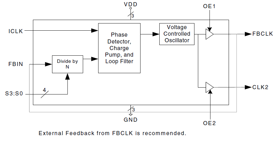
The ICS670-03 is a high speed, low phase noise, Zero Delay Buffer (ZDB) which integrates IDT’s proprietary analog/digital Phase Locked Loop (PLL) techniques. It is identical to the ICS670-01, but with an increased maximum output frequency of 210 MHz. Part of IDT’s ClockBlocks family, the part’s zero delay feature means that the risingedge of the input clock aligns with the rising edges of the
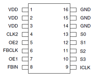
outputs giving the appearance of no delay through the device. There are two identical outputs on the chip. The FBCLK should be used to connect to the FBIN. Each output has its own output enable pin.
The ICS670-03 is ideal for synchronizing outputs in a large variety of systems, from personal computers to data communications to video. By allowing off-chip feedback paths, the ICS670-03 can eliminate the delay through other devices. The 15 different on-chip multipliers work in a variety of applications. For other multipliers, including functional multipliers, see the ICS527.