パッケージ情報
| CADモデル: | View CAD Model |
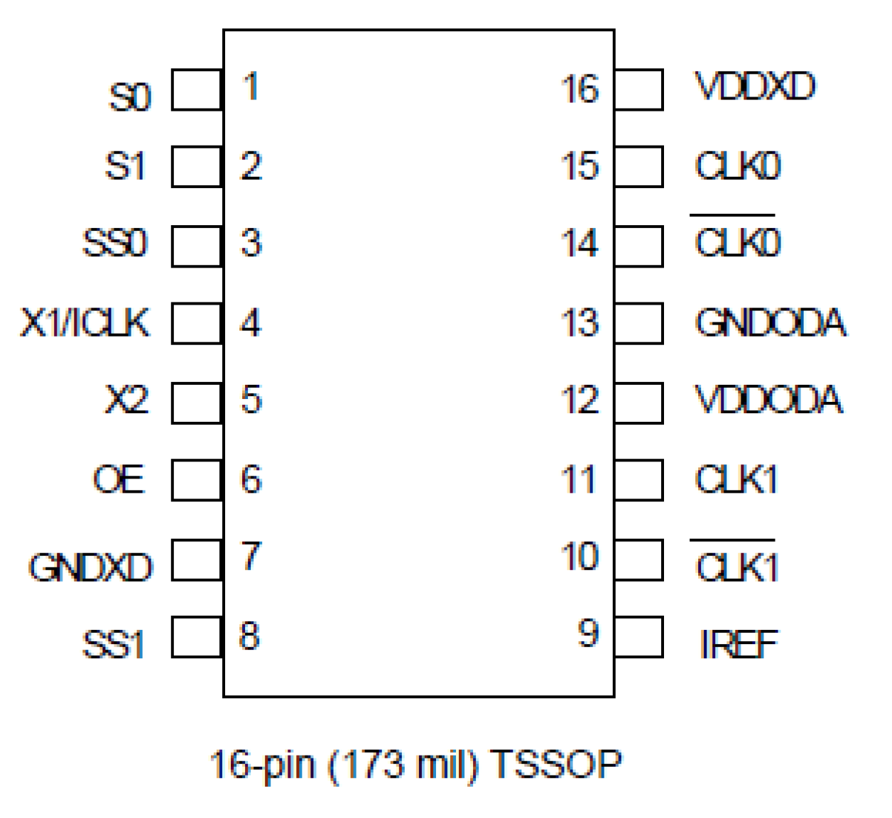
| Pkg. Type: | TSSOP |
| Pkg. Code: | PGG16 |
| Lead Count (#): | 16 |
| Pkg. Dimensions (mm): | 5.0 x 4.4 x 1.0 |
| Pitch (mm): | 0.65 |
環境及び輸出分類情報
| Pb (Lead) Free | Yes |
| ECCN (US) | EAR99 |
| HTS (US) | 8542.39.0090 |
| Moisture Sensitivity Level (MSL) | 1 |
製品スペック
| Pkg. Type | TSSOP |
| Lead Count (#) | 16 |
| Pb (Lead) Free | Yes |
| Carrier Type | Tube |
| Advanced Features | Spread Spectrum |
| App Jitter Compliance | PCIe Gen1 |
| Architecture | Common |
| C-C Jitter Max P-P (ps) | 80 |
| Core Voltage (V) | 3.3 |
| Diff. Output Signaling | HCSL |
| Diff. Outputs | 2 |
| Diff. Termination Resistors | 8 |
| Feedback Input | No |
| Input Freq (MHz) | 25 - 25 |
| Input Type | Crystal, LVCMOS |
| Inputs (#) | 1 |
| Length (mm) | 5 |
| MOQ | 384 |
| Moisture Sensitivity Level (MSL) | 1 |
| Output Banks (#) | 1 |
| Output Freq Range (MHz) | 25 - 25, 100 - 100, 125 - 125, 200 - 200 |
| Output Skew (ps) | 50 |
| Output Type | HCSL |
| Output Voltage (V) | 3.3 |
| Outputs (#) | 2 |
| PLL | Yes |
| Package Area (mm²) | 22 |
| Pb Free Category | e3 Sn |
| Pitch (mm) | 0.65 |
| Pkg. Dimensions (mm) | 5.0 x 4.4 x 1.0 |
| Power Consumption Typ (mW) | 132 |
| Prog. Clock | No |
| Qty. per Carrier (#) | 96 |
| Qty. per Reel (#) | 0 |
| Reference Output | No |
| Requires Terms and Conditions | Does not require acceptance of Terms and Conditions |
| Spread Spectrum | Yes |
| Supply Voltage (V) | 3.3 - 3.3 |
| Tape & Reel | No |
| Temp. Range (°C) | -40 to 85°C |
| Thickness (mm) | 1 |
| Width (mm) | 4.4 |
| Xtal Freq (MHz) | 25 - 25 |
5V41129 に関するリソース
説明
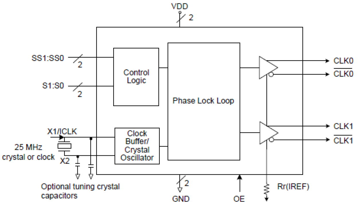
The IDT5V41129 is a spread spectrum clock generator that supports PCI-Express Gen1 and Ethernet requirements.The device is used for PC or embedded systems to substantially reduce electromagnetic interference (EMI). The device provides two differential (HCSL) spread spectrum outputs. The spread type and amount are configured via select pin. Using IDT’s patented Phase-Locked Loop (PLL) techniques, the device takes a 25 MHz crystal input and produces two pairs of differential outputs at 25 MHz, 100 MHz, 125 MHz or 200 MHz clock frequencies for HCSL, and 25 MHz or 100 MHz for LVDS.


