
特長
- Ref input is 3.3V tolerant
- 8 pairs of programmable skew outputs
- Low skew: 185ps same pair, 250ps same bank, 350ps both banks
- Selectable positive or negative edge synchronization on each bank: excellent for DSP applications
- Synchronous output enable on each bank
- Input frequency: 2MHz to 160MHz
- Output frequency: 6MHz to 160MHz
- 3-level inputs for skew and PLL range control
- 3-level inputs for feedback divide selection multiply / divide ratios of (1-6, 8, 10, 12) / (2, 4)
- PLL bypass for DC testing
- External feedback, internal loop filter
- 12mA balanced drive outputs
- Low Jitter: <100ps cycle-to-cycle
- Power-down mode on each bank
- Lock indicator on each bank
- Available in BGA package
- Not Recommended for New Design
説明
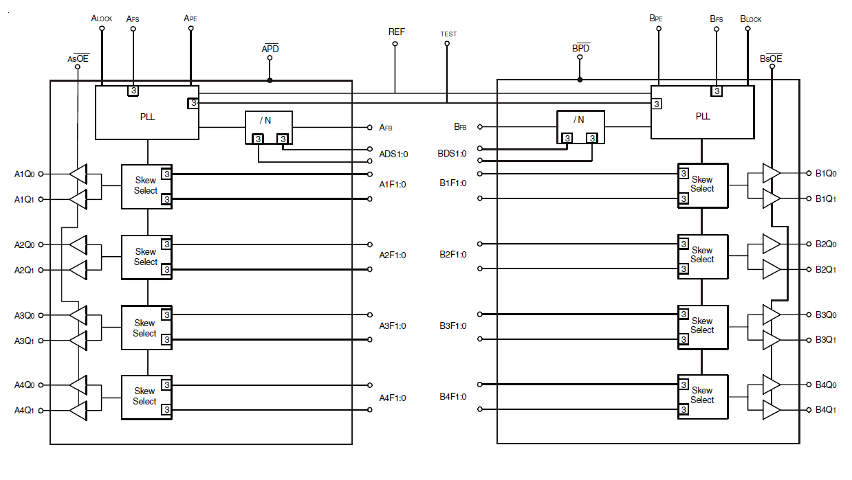
The 5T9955 is a high fanout 2.5V PLL based clock driver intended for high performance computing and data-communications applications. A key feature of the programmable skew is the ability of outputs to lead or lag the REF input signal. The 5T9955 has sixteen programmable skew outputs in eight banks of 2. The two separate PLLs allow the user to independently control A and B banks. Skew is controlled by 3-level input signals that may be hard-wired to appropriate high-mid-low levels. The feedback input allows divide-by-functionality from 1 to 12 through the use of the xDS[1:0] inputs. This provides the user with frequency multiplication from 1 to 12 without using divided outputs for feedback. When the xsOE pin is held low, all the xbank outputs are synchronously enabled. However, if xsOE is held high, all the xbank outputs except x2Q0 and x2Q1 are synchronously disabled. The xLOCK output is high when the xbank PLL has achieved phase lock. Furthermore, when xPE is held high, all the outputs are synchronized with the positive edge of the REF clock input. When xPE is held low, all the outputs are synchronized with the negative edge of REF. The 5T9955 has LVTTL outputs with 12mA balanced drive outputs.


