
| CADモデル: | View CAD Model |
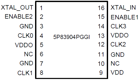
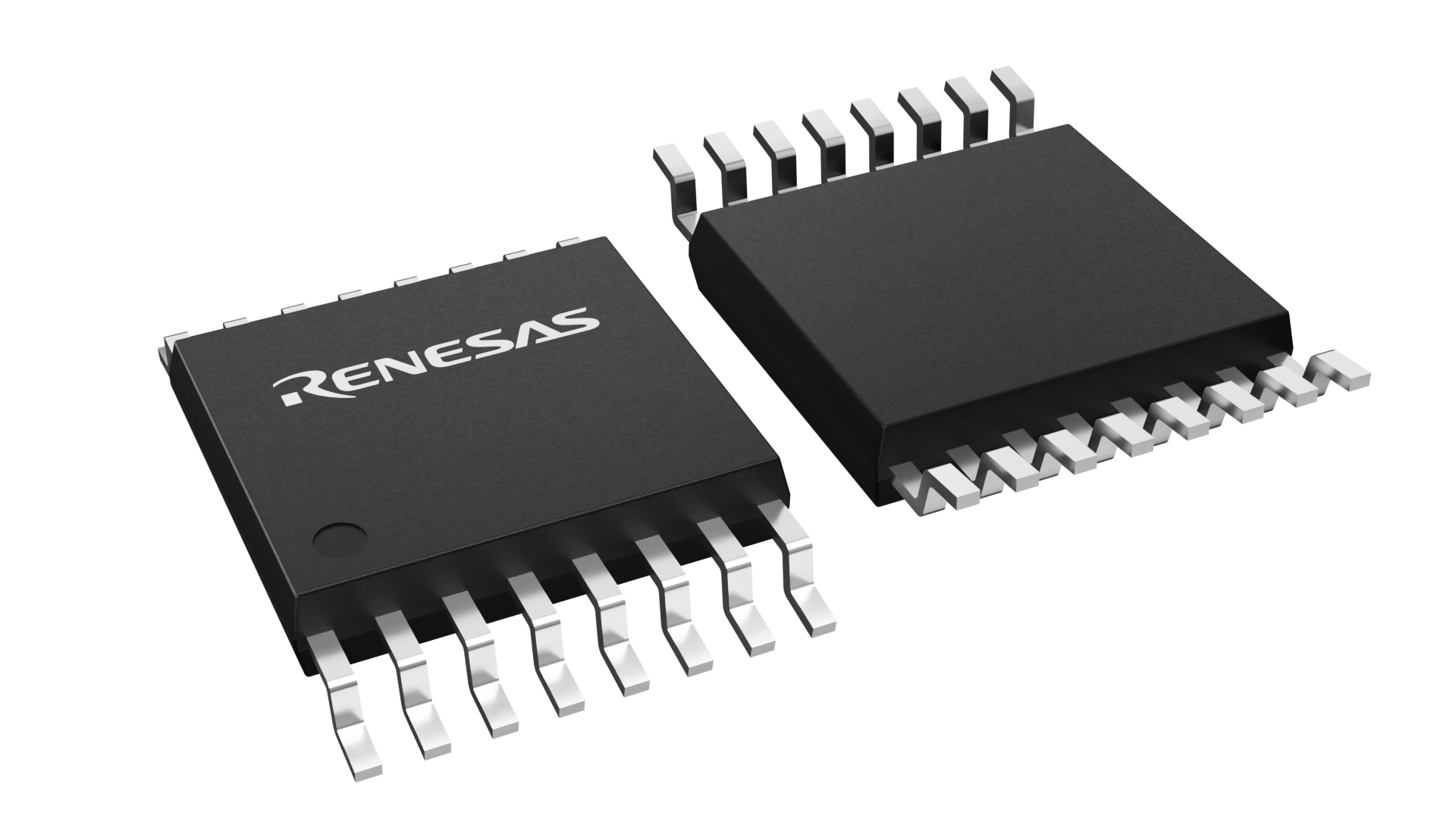
| Pkg. Type: | TSSOP |
| Pkg. Code: | PGG16 |
| Lead Count (#): | 16 |
| Pkg. Dimensions (mm): | 5.0 x 4.4 x 1.0 |
| Pitch (mm): | 0.65 |
| Moisture Sensitivity Level (MSL) | 1 |
| Pb (Lead) Free | Yes |
| ECCN (US) | EAR99 |
| HTS (US) | 8542.39.0090 |
| Lead Count (#) | 16 |
| Carrier Type | Reel |
| Moisture Sensitivity Level (MSL) | 1 |
| Qty. per Reel (#) | 2500 |
| Package Area (mm²) | 22 |
| Pitch (mm) | 0.65 |
| Pkg. Dimensions (mm) | 5.0 x 4.4 x 1.0 |
| Reel Size (in) | 13 |
| Qty. per Carrier (#) | 0 |
| Pb (Lead) Free | Yes |
| Pb Free Category | e3 Sn |
| Temp. Range (°C) | -40 to 105°C |
| Assembly Location | TAIWAN |
| Wafer Fab Location | TAIWAN |
| Additive Phase Jitter Typ RMS (fs) | 50 |
| Core Voltage (V) | 1.8V, 2.5V, 3.3V |
| Function | Buffer |
| Input Freq (MHz) | 200 |
| Input Type | Crystal, LVCMOS |
| Inputs (#) | 1 |
| Length (mm) | 5 |
| MOQ | 2500 |
| Output Banks (#) | 1 |
| Output Freq Range (MHz) | 200 |
| Output Signaling | LVCMOS |
| Output Skew (ps) | 65 |
| Output Type | LVCMOS |
| Output Voltage (V) | 1.8V, 2.5V, 3.3V |
| Outputs (#) | 4 |
| Pkg. Type | TSSOP |
| Product Category | Clock Buffers & Drivers |
| Reference Output | Yes |
| Requires Terms and Conditions | Does not require acceptance of Terms and Conditions |
| Spread Spectrum | No |
| Tape & Reel | Yes |
| Thickness (mm) | 1 |
| Width (mm) | 4.4 |
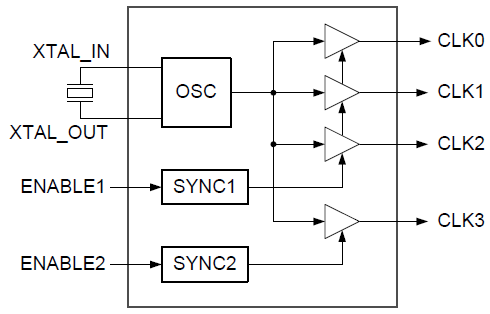
The 5P83904 is a high-performance, 1-to-4 crystal input to LVCMOS fanout buffer with output enable pins. This device accepts a fundamental mode crystal from 10MHz to 40MHz and outputs LVCMOS clocks with best-in-class phase noise performance.
The 5P83904 features a synchronous glitch-free Output Enable function to eliminate any intermediate incorrect output clock cycles when enabling or disabling outputs. It comes in standard TSSOP packages or small QFN packages and can operate from 1.8V to 3.3V supplies.