
| CADモデル: | View CAD Model |
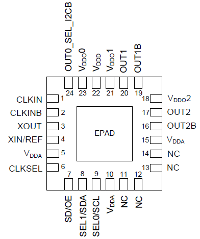
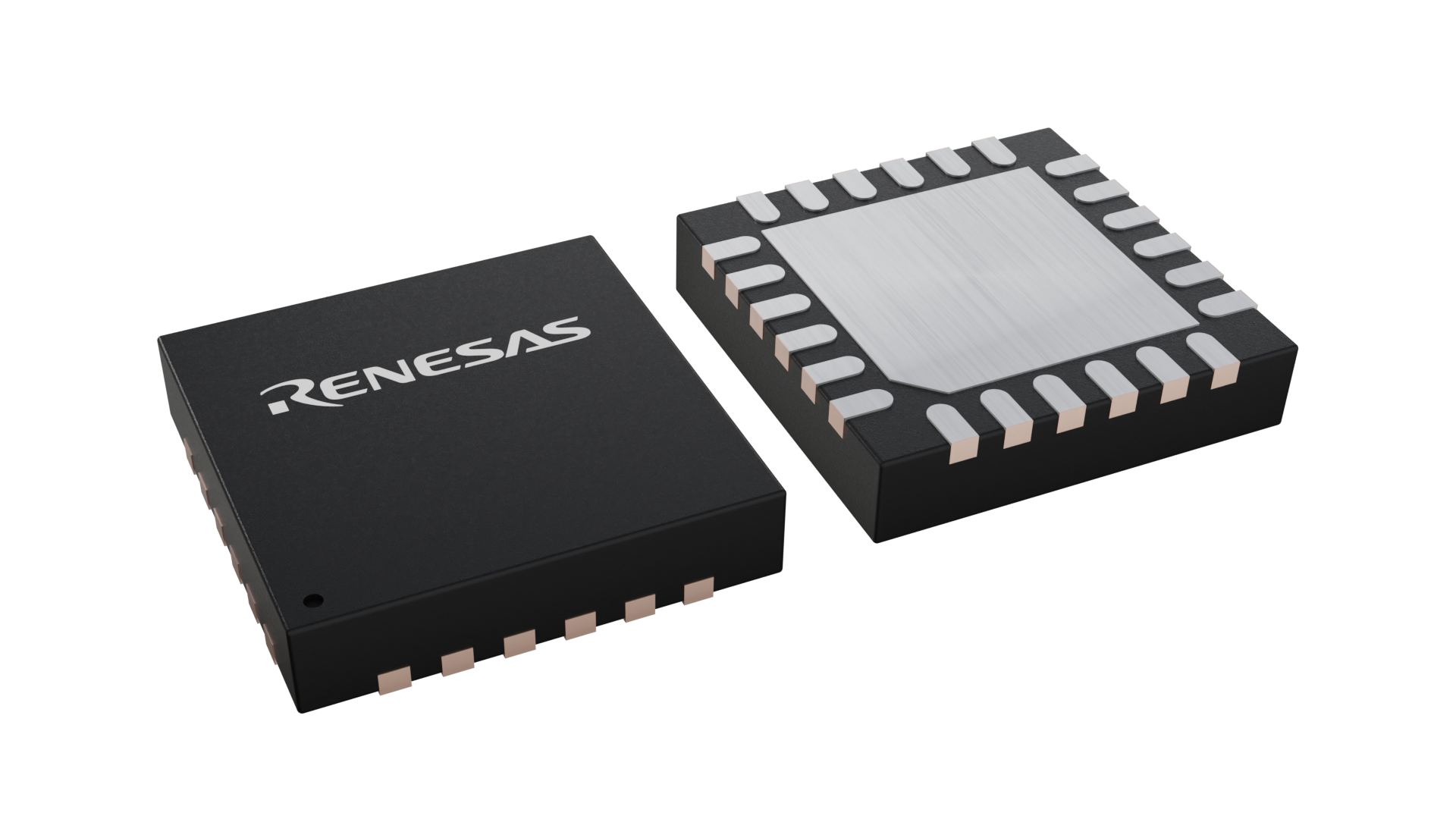
| Pkg. Type: | VFQFPN |
| Pkg. Code: | NLG24 |
| Lead Count (#): | 24 |
| Pkg. Dimensions (mm): | 4.0 x 4.0 x 0.9 |
| Pitch (mm): | 0.5 |
| Moisture Sensitivity Level (MSL) | 1 |
| Pb (Lead) Free | Yes |
| ECCN (US) | EAR99 |
| HTS (US) | 8542.39.0090 |
| Lead Count (#) | 24 |
| Carrier Type | Tray |
| Moisture Sensitivity Level (MSL) | 1 |
| Qty. per Reel (#) | 0 |
| Qty. per Carrier (#) | 490 |
| Pb (Lead) Free | Yes |
| Pb Free Category | e3 Sn |
| Temp. Range (°C) | -40 to 85°C |
| Country of Assembly | MALAYSIA, TAIWAN |
| Country of Wafer Fabrication | SINGAPORE |
| Additive Phase Jitter Typ RMS (ps) | 0.2 |
| Core Voltage (V) | 1.8V, 2.5V, 3.3V |
| Function | Buffer, Multiplexer |
| Input Freq (MHz) | 1 - 350 |
| Input Type | Crystal, LVCMOS, LVPECL, LVDS, HCSL |
| Inputs (#) | 2 |
| Length (mm) | 4 |
| MOQ | 490 |
| Output Banks (#) | 3 |
| Output Freq Range (MHz) | 1 - 350 |
| Output Skew (ps) | 35 |
| Output Type | LVCMOS, LVPECL, LVDS, HCSL |
| Output Voltage (V) | 1.8V, 2.5V, 3.3V |
| Outputs (#) | 3 |
| Package Area (mm²) | 16 |
| Pitch (mm) | 0.5 |
| Pkg. Dimensions (mm) | 4.0 x 4.0 x 0.9 |
| Pkg. Type | VFQFPN |
| Price (USD) | $2.44848 |
| Product Category | Clock Buffers & Drivers, Clock Multiplexers |
| Prog. Interface | I2C, Pin select |
| Requires Terms and Conditions | Does not require acceptance of Terms and Conditions |
| Tape & Reel | No |
| Thickness (mm) | 0.9 |
| Width (mm) | 4 |
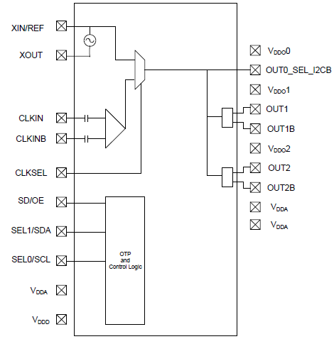
The 5P1103 is a programmable fanout buffer intended for high-performance consumer, networking, industrial, computing, and data communications applications. Configurations may be stored in on-chip One-Time Programmable (OTP) memory or changed using the I²C interface.
The outputs are generated from a single reference clock. The input reference can be a crystal, external single-ended, or differential clock. The reference clock can come from one of the two redundant clock inputs and is selected by the CLKSEL pin. A glitchless manual switchover function allows one of the redundant clocks to be selected during normal operation. Two select pins allow up to four different configurations to be programmed and accessible using processor GPIOs or bootstrapping. The device is available in a 24-pin VFQFPN 4mm x 4mm package, with an industrial operating temperature range of -40 °C to +85 °C.
