

| CADモデル: | View CAD Model |
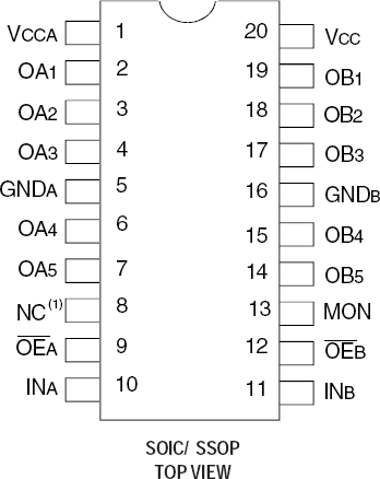
| Pkg. Type: | SSOP |
| Pkg. Code: | PYG20 |
| Lead Count (#): | 20 |
| Pkg. Dimensions (mm): | 7.2 x 5.3 x 1.73 |
| Pitch (mm): | 0.65 |
| Moisture Sensitivity Level (MSL) | 1 |
| Pb (Lead) Free | Yes |
| ECCN (US) | EAR99 |
| HTS (US) | 8542.39.0090 |
| Lead Count (#) | 20 |
| Carrier Type | Tube |
| Moisture Sensitivity Level (MSL) | 1 |
| Qty. per Reel (#) | 0 |
| Qty. per Carrier (#) | 64 |
| Package Area (mm²) | 38.2 |
| Pitch (mm) | 0.65 |
| Pkg. Dimensions (mm) | 7.2 x 5.3 x 1.73 |
| Pb (Lead) Free | Yes |
| Pb Free Category | e3 Sn |
| Temp. Range (°C) | 0 to 70°C |
| Core Voltage (V) | 5 |
| Function | Buffer |
| Input Type | LVCMOS |
| Inputs (#) | 2 |
| Length (mm) | 7.2 |
| MOQ | 192 |
| Output Banks (#) | 2 |
| Output Skew (ps) | 700 |
| Output Type | LVCMOS |
| Output Voltage (V) | 5 |
| Outputs (#) | 10 |
| Pkg. Type | SSOP |
| Product Category | Clock Buffers & Drivers |
| Requires Terms and Conditions | Does not require acceptance of Terms and Conditions |
| Tape & Reel | No |
| Thickness (mm) | 1.73 |
| Width (mm) | 5.3 |
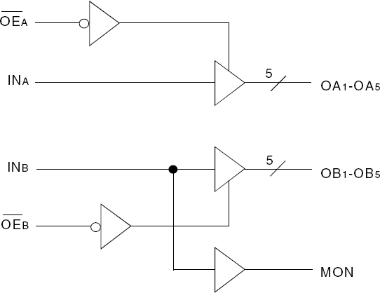
The 49FCT805 is a non-inverting buffer/clock driver built using advanced dual metal CMOS technology. Each bank consists of two banks of drivers. Each bank drives five output buffers from a standard TTL compatible input. These devices feature a "heart-beat" monitor for diagnostics and PLL driving. The MON output is identical to all other outputs and complies with the output specifications in this document. The 49FCT805 offers low capacitance inputs and hysteresis. Rail-to-rail output swing improves noise margin and allows easy interface with CMOS inputs.