
| CADモデル: | View CAD Model |
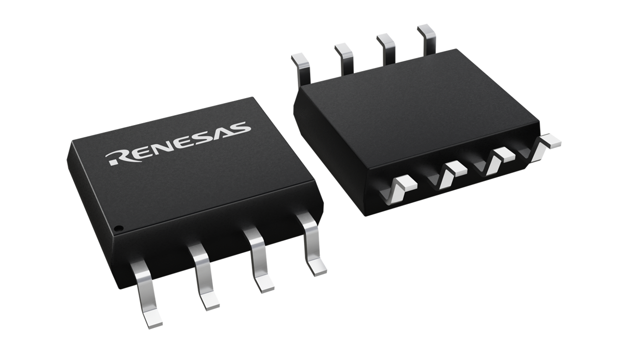
| Pkg. Type: | SOIC |
| Pkg. Code: | DCG8 |
| Lead Count (#): | 8 |
| Pkg. Dimensions (mm): | 4.9 x 3.9 x 1.5 |
| Pitch (mm): | 1.27 |
| Moisture Sensitivity Level (MSL) | 1 |
| Pb (Lead) Free | Yes |
| ECCN (US) | EAR99 |
| HTS (US) | 8542.39.0090 |
| Lead Count (#) | 8 |
| Carrier Type | Tube |
| Moisture Sensitivity Level (MSL) | 1 |
| Qty. per Reel (#) | 0 |
| Qty. per Carrier (#) | 97 |
| Pb (Lead) Free | Yes |
| Pb Free Category | e3 Sn |
| Temp. Range (°C) | 0 to 70°C |
| Advanced Features | Programmable Clock, Spread Spectrum, Reference Output |
| Core Voltage (V) | 3.3 |
| Family Name | VersaClock |
| Input Freq (MHz) | 2 - 150 |
| Input Type | Crystal, LVCMOS |
| Inputs (#) | 1 |
| Length (mm) | 4.9 |
| MOQ | 291 |
| Output Banks (#) | 1 |
| Output Freq Range (MHz) | 0.314 - 200 |
| Output Type | LVCMOS |
| Output Voltage (V) | 3.3 |
| Outputs (#) | 2 |
| Package Area (mm²) | 19.1 |
| Period Jitter Typ P-P (ps) | 200 |
| Phase Jitter Typ RMS (fs) | 50000 |
| Phase Jitter Typ RMS (ps) | 50 |
| Pitch (mm) | 1.27 |
| Pkg. Dimensions (mm) | 4.9 x 3.9 x 1.5 |
| Pkg. Type | SOIC |
| Product Category | VersaClock, Programmable Clocks |
| Prog. Clock | Yes |
| Prog. Interface | OTP |
| Reference Output | Yes |
| Requires Terms and Conditions | Does not require acceptance of Terms and Conditions |
| Spread Spectrum | Yes |
| Tape & Reel | No |
| Thickness (mm) | 1.5 |
| Width (mm) | 3.9 |
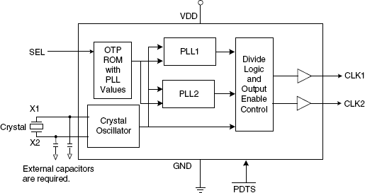
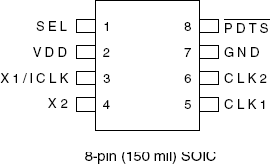
The 252 is a low cost, dual-output, field programmable clock synthesizer. The 252 can generate two output frequencies from 314 kHz to 200 MHz using up to two independently configurable PLLs. The outputs may employ Spread Spectrum techniques to reduce system electro-magnetic interference (EMI). Using IDT's VersaClock™ software to configure the PLL and output, the 252 contains a One-Time Programmable (OTP) ROM to allow field programmability. Programming features include 2 selectable configuration registers. The device employs Phase-Locked Loop (PLL) techniques to run from a standard fundamental mode, inexpensive crystal, or clock. It can replace multiple crystals and oscillators, saving board space and cost. The device also has a power-down feature that tri-states the clock outputs and turns off the PLLs when the PDTS pin is taken low. The 252 is also available in factory programmed custom versions for high-volume applications.