
| CADモデル: | View CAD Model |
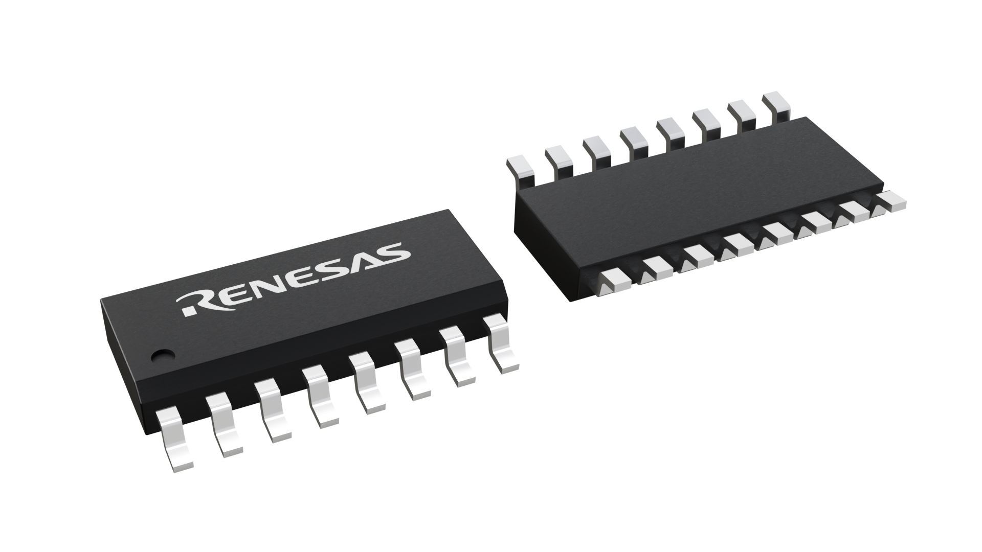
| Pkg. Type: | SOIC |
| Pkg. Code: | DCG16 |
| Lead Count (#): | 16 |
| Pkg. Dimensions (mm): | 9.9 x 3.9 x 1.5 |
| Pitch (mm): | 1.27 |
| Moisture Sensitivity Level (MSL) | 3 |
| Pb (Lead) Free | Yes |
| ECCN (US) | EAR99 |
| HTS (US) | 8542.39.0090 |
| Lead Count (#) | 16 |
| Carrier Type | Reel |
| Moisture Sensitivity Level (MSL) | 3 |
| Qty. per Carrier (#) | 0 |
| Package Area (mm²) | 38.6 |
| Pitch (mm) | 1.27 |
| Pkg. Dimensions (mm) | 9.9 x 3.9 x 1.5 |
| Qty. per Reel (#) | 2500 |
| Pb (Lead) Free | Yes |
| Pb Free Category | e3 Sn |
| Temp. Range (°C) | 0 to 70°C |
| Assembly Location | TAIWAN |
| Wafer Fab Location | TAIWAN, USA |
| C-C Jitter Max P-P (ps) | 200 |
| Core Voltage (V) | 3.3 |
| Feedback Input | No |
| Input Freq (MHz) | 10 - 133 |
| Input Type | LVCMOS |
| Inputs (#) | 1 |
| Length (mm) | 9.9 |
| MOQ | 2500 |
| Output Banks (#) | 3 |
| Output Freq Range (MHz) | 10 - 133 |
| Output Skew (ps) | 250 |
| Output Type | LVCMOS |
| Output Voltage (V) | 3.3 |
| Outputs (#) | 9 |
| Pkg. Type | SOIC |
| Product Category | Zero Delay Buffers |
| Prog. Clock | No |
| Reel Size (in) | 13 |
| Requires Terms and Conditions | Does not require acceptance of Terms and Conditions |
| Tape & Reel | Yes |
| Thickness (mm) | 1.5 |
| Width (mm) | 3.9 |
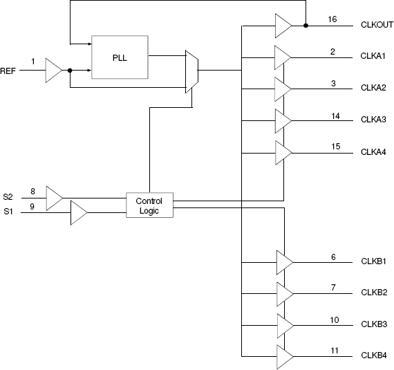
The 2309A is a high-speed phase-lock loop (PLL) clock buffer, designed to address high-speed clock distribution applications. The zero delay is achieved by aligning the phase between the incoming clock and the output clock, operable within the range of 10 to 133MHz. The 2309A is a 16-pin version of the 2305A. The 2309A accepts one reference input, and drives two banks of four low skew clocks. The -1H version of this device operates up to 133MHz frequency and has higher drive than the -1 device. All parts have on-chip PLLs which lock to an input clock on the REF pin. The PLL feedback is on-chip and is obtained from the CLKOUT pad. In the absence of an input clock, the 2309A enters power down. In this mode, the device will draw less than 12uA for Commercial Temperature range and less than 25uA for Industrial temperature range, and the outputs are tri-stated. The 2309A is characterized for both Industrial and Commercial operation.