Pulse width modulation (PWM) is utilized to control the input to the associated power switch and reduce output capacitance.
Multiphase Power Conversion
Designing a regulator that is cost-effective, thermally sound and efficient has become a challenge that only multiphase converters can accomplish. Switch-mode DC/DC converters require a means to vary their output voltage in response to changes in their load. Pulse width modulation (PWM) is utilized to control the input to the associated power switch and reduce output capacitance.
More voltage rails in a system lead to more complex power management needs. Renesas's multiphase modulation technology comes from our experience in analog multiphase controllers used in computing, but is becoming applicable to a much larger set of applications. Our ICs can react to loads at very high speeds, are highly efficient and have evolved into much smaller form factors to drive innovation in the digital market.
Dual-Edge PWM Improves Multiphase Regulators
Transient response is a key performance parameter for the multiphase voltage regulator, especially in microprocessor applications. Conventional pulse width modulation schemes have delay times that can increase the demand on the output capacitors, forcing designs to employ more capacitors for acceptable performance.
Active Pulse Positioning (APP) Modulated PWM Operation
Conventional pulse width modulation schemes have delay times that can increase the demand on the output capacitors, forcing designs to employ more capacitors for acceptable performance. Renesas's approach to PWM, known as Active Pulse Positioning (APP), achieves very fast transient response by dramatically reducing the modulator delay time. This modulation scheme adopts two separate ramp signals to control both the leading edge and trailing edge of the PWM pulse. Controller ICs that implement APP modulation can respond to transient events immediately and require much less output capacitance than other modulators.
Regulating Dynamic Loads
With fast transient response, less output capacitance is needed to meet the design specifications for the regulator. For most applications, the output voltage will drop to its minimum value in several switching cycles after the step load is applied and then settle to its final value slowly. For these applications, increasing the closed-loop bandwidth is important for fast transient response.
This situation is compounded for multiphase voltage regulators for microprocessor core power applications. The current drawn by modern microprocessors is highly dynamic with a wide-varying transient duration and repetition rate. The typical step-load current can be as high as 100A with a slew rate up to 1,000Aµs. To address this demand, the voltage regulator needs its output voltage to settle rapidly after the transient event in order to be ready for the next transient event.
Adaptive Voltage Positioning (AVP) control, also referred to as droop control or load-line control is a popular scheme used to power today's microprocessors. With this control, the output voltage will be reduced in proportion to the load current; the output voltage at heavy load is lower than that at light load, resulting in more cost-effective transient-load regulation. The output voltage after the step load does not need to return to its original value, resulting in much shorter settling time.
The typical response and settling time for the voltage regulator with AVP control is only a few microseconds in typical microprocessor core regulators. With a typical 300kHz switching frequency, this means the transient event can occur and the regulator must respond completely within one switching cycle. Therefore, any delay in the system will have significant impact on the transient response, and the conventional loop bandwidth concept is not adequate for analyzing the regulator performance. Instead, it is necessary to investigate and reduce the delays in the entire system to improve the transient performance.
Limitations of Conventional PWM
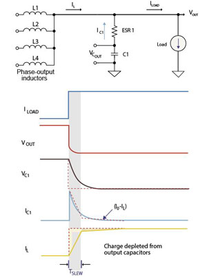
Assuming that the high-voltage spike caused by the bulk-capacitor equivalent series inductance (ESL) is absorbed by the high-frequency ceramic capacitors, the capacitor equivalent series resistance (ESR) and the inductor current slew rate become the main factors that impact the transient performance. When the load step is applied to the voltage regulator, the output voltage will drop immediately and the initial voltage drop depends on the ESR of the output capacitor. AVP control will regulate the output voltage to the new value based on the output current.
During the settling time, the output capacitor is discharged to provide some portions of the load current, while the inductor current increases in response to the larger load current. When the inductor current slew rate matches that of the discharging current from the output capacitor, the output voltage waveform can approach an ideal square wave, if desired. Thus, with an increase to the total inductor current slew rate, the current demand on the output capacitors will be reduced and less output capacitance will be required.
There are two parameters that determine the time for the total inductor current to ramp up to the load current: the delay time of the PWM pulses and the slew rate of the total inductor current. To reduce the delay of the PWM pulses, the PWM modulator should respond to the error amplifier voltage change as soon as possible. For a given system, the phase inductor current slew rate is fixed, set by the input voltage, output voltage and inductance.
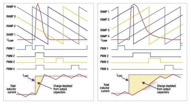
To obtain a faster total inductor current slew rate, more than one phase can be turned on simultaneously. This requires the PWM modulator to allow phase overlap and turn on additional phases proportionally to the step load. Based on these observations, the PWM modulator plays an important role in achieving fast transient response.
Conversely, the leading-edge modulation scheme has an excellent turn-on response but a poor turn-off response. Conventional dual-edge modulation, based on a triangular-ramp waveform, provides significant improvements over either of the single-edge schemes, but can still have half-switching-cycle delays for the turn-on and turn-off edges. Based on this observation, the APP PWM scheme is introduced to minimize both turn-on and turn-off delays by combining the benefits of the trailing-edge and leading-edge modulators.
Reducing Output Capacitance
To increase the inductor current slew rate in multiphase applications, it is preferred that more than one phase be turned on simultaneously, based on the transient step load. The APP scheme is excellent for this demand. All phases are turned on when VCOMP jumps very high in response to a large output-voltage change associated with a high di/dt load step. Since the total inductor current increases very fast and reaches the load current quickly, the current drawn from output capacitors is reduced. The voltage regulator with the conventional trailing-edge modulation scheme will need more output capacitors to provide additional current when the total inductor current increases slowly. A similar case could be examined for leading-edge modulation on a load stepdown.
Renesas has introduced a family of multiphase controllers based on the APP modulator that enables higher performance and lower cost than traditional multiphase modulators.
With the APP modulator, the transient response of the voltage regulator is improved significantly. Without extra delay and an extremely fast transient response, the switching frequency can be reduced to increase efficiency without sacrificing transient performance. Due to the simultaneous all-phase-on feature, larger-output inductors can be used to reduce the ripple phase current. Or, with the same output inductor, the output capacitors can be reduced to meet the same transient requirement. Furthermore, the benefits of using coupled inductors can be further improved with the APP modulator. Typically, ceramic capacitors are used to absorb the initial voltage spike caused by the fast load current slew rate and the ESL impact of the bulk capacitors. Therefore the selection of the ceramic capacitor is similar to that of the conventional voltage regulator. However, the fast current slew rate of the total inductor current during a transient event will reduce the demand on the bulk capacitor ESR. Therefore, a less-expensive bulk capacitor solution can be employed in the voltage regulator with the APP modulator.
Enhanced Active Pulse Positioning (EAPP)
Renesas's proprietary EAPP modulation scheme enables extremely fast transient response with fewer output capacitors. Our multiphase controllers include programmable functions and telemetrics for easy use, high system flexibility and overclocking applications using SMBus, PMBus or an I2C interface. Featured with R3/R4 and EAPP modulation schemes, Renesas processor power products have been extensively verified in customer designs, with super-fast load transient response, precise current balance under all load conditions and excellent stability.
Explore our PWM Products
The graph shows a comparison between APP modulation (left) and conventional trailing-edge modulation (right) schemes used in a multiphase regulator; it reveals that the total inductor current can increase more rapidly with the APP scheme, reducing the demand on the output capacitor.
PowerCompass
The PowerCompassTM tool helps you design your power supply in minutes, giving you tools to find Renesas parts that match your requirements, set up multiple rails if needed, perform high-level system analysis and generate reference design files.
PowerCompass supports over 200 FPGAs, including built-in templates for Xilinx FPGA families. You can even save time by importing Xilinx Power Estimator output files to get system efficiency and power dissipation projections.
Documentation
|
|
|
|
|---|---|---|
| Type | Title | Date |
| White Paper |
PDF
322 KB
简体中文
Power systems with modern processors require low output voltages and fast switching frequencies. This paper explores narrow on-time point-of-load conversion challenges and compares current mode control methods. It introduces a hybrid valley current mode architecture that enables direct 48V to 1V conversion while maintaining stability and reducing design complexity.
|
|
1 item
|
||
