
特長
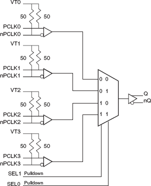
- High speed differential multiplexer. The device can be configured as either a 4:1 or 2:1 multiplexer
- One LVDS output pair
- Four selectable PCLK, nPCLK inputs with internal termination
- PCLKx, nPCLKx pairs can accept the following differential input levels: LVPECL, LVDS, CML, SSTL
- Maximum output frequency: >2GHz
- Part-to-part skew: 200ps (maximum)
- Propagation delay: 800ps (maximum)
- Additive phase jitter, RMS: 0.065ps (typical)
- Full 2.5V power supply
- -40°C to 85°C ambient operating temperature
- Available in lead-free (RoHS 6) package
説明
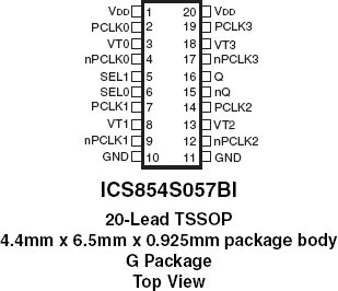
The 854S057BI is a 4:1 or 2:1 LVDS Clock Multiplexer which can operate up to 2GHz. The PCLK, nPCLK pairs can accept most standard differential input levels. Internal termination is provided on each differential input pair. The 854S057BI operates using a 2.5V supply voltage. The fully differential architecture and low propagation delay make it ideal for use in high speed multiplexing applications. The select pins have internal pulldown resistors. Leaving one input unconnected (pulled to logic low by the internal resistor) will transform the device into a 2:1 multiplexer. The SEL1 pin is the most significant bit and the binary number applied to the select pins will select the same numbered data input (i.e., 00 selects PCLK0, nPCLK0).