TOKYO, Japan ― Renesas Electronics Corporation (TSE: 6723), a premier supplier of advanced semiconductor solutions, today announced the development of new low-power technology for use in embedded flash memory based on a 65 nanometer (nm) SOTB™ (Silicon On Thin Buried Oxide) process. Available with 1.5 MB capacity, it is the world’s first embedded 2T-MONOS (2 Transistors-Metal Oxide Nitride Oxide Silicon) flash memory based on 65nm SOTB technology (Note 1). With the addition of a new circuit technology that reduces the power consumption of the peripheral circuits on flash memory, Renesas achieves read energy as low as 0.22 picojoules per bit (pJ/bit) at an operating frequency of 64 MHz – among the world’s lowest levels for embedded flash memory on an MCU. The newly developed low-power technology for peripheral circuits comprises circuit technology that (1) reduces energy consumption when sensing data in memory and (2) reduces the amount of transmission energy consumed when read data is transmitted to an external destination. Together, these advances substantially reduce energy consumption when reading data from the memory.
Renesas presented these results on June 12 at the 2019 Symposia on VLSI Technology and Circuits in Kyoto, Japan, June 9-14, 2019.
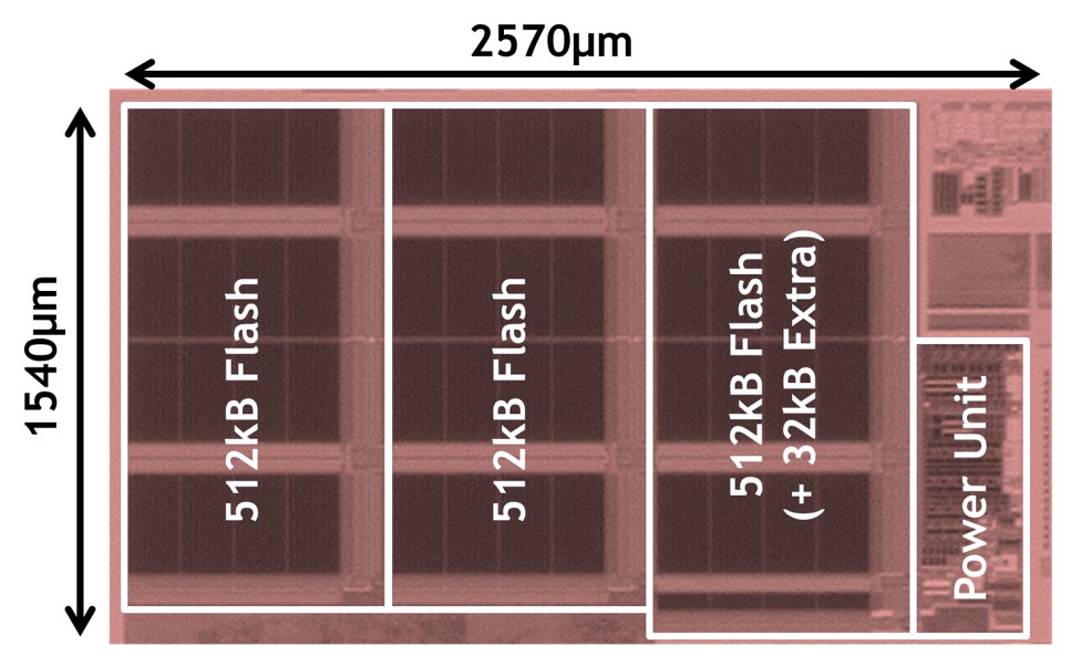
The new SOTB-based technology has already been implemented in the Renesas R7F0E embedded controller, which is intended specifically for energy harvesting applications. Renesas’ exclusive SOTB process technology dramatically reduces power consumption in both the active and standby states. Power consumption in these two states had previously been a tradeoff: Lower power consumption in one generally meant higher power consumption in the other. The new technology substantially reduces power consumption when reading data from the flash memory. In contrast to non-SOTB 2T-MONOS flash memory, which requires a memory read current of about 50 µA/MHz, the read current is reduced to a mere approximately 6 µA/MHz. This is equivalent to a read energy level of 0.22 pJ/bit, one of the lowest levels for embedded flash memory on an MCU. The new technology also contributes greatly to the achievement of a low-active read current of 20 µA/MHz on the R7F0E, among the best in the industry.
Key Features of the Newly Developed Embedded Flash Memory Technology:
Low-power 2T-MONOS flash memory ideally suited to the SOTB process
The 2T-MONOS embedded flash memory using the SOTB process has a two-transistor structure comprising electrically isolated elements. Unlike a single-transistor structure, there is no need for negative voltage during read operation, and this reduces power consumption when reading data. In addition, compared with other memory processes, MONOS uses fewer masks during the production process, and it is possible to store data with a discrete charge-trapping scheme. This enables low power consumption and high rewrite reliability without increasing the production cost.
Sense amplifier circuit and regulator circuit technology for ultra-low energy consumption
Most of the energy consumption during memory read operations occurs during sensing operation to identify data and transmit operation to output the identified data to an external destination. To address the former, a single-ended sense amplifier substantially reduces the bit line pre-charge energy during sensing operation, employing a new charge-transfer technology that boosts pre-charging speed and energy efficiency. In addition, a newly developed regulator circuit technology uses leak monitoring to perform optimal intermittent control of the sense amplifier’s reference voltage which consumes energy in a constant manner. These advances make it possible to speed up sensing operation while substantially reducing energy consumption.
Circuit technology that dramatically cuts data transmission energy consumption
One characteristic of the SOTB process is minimal variation in the transistor threshold (Vth), and the newly developed circuit technology takes advantage of this to achieve data transmission using an extremely small voltage amplitude. This advance results in a substantial decrease in the transmission energy consumed when read data transmitted to an external destination.
By helping to make endpoint devices more intelligent, Renesas is accelerating the trend toward a “smart society.” Renesas considers energy harvesting systems, which do not need batteries and therefore never require battery replacement, to be an essential step toward this goal, and plans to continue developing technology that will help to realize an environmentally friendly smart society.
(Note 1) MONOS: Metal-oxide-nitride-oxide-silicon. Renesas has achieved a substantial track record with MONOS technology over the past 20 years in EEPROM, secure MCU, and other products. The MONOS technology is used in the embedded flash memory of Renesas MCUs.
About Renesas Electronics Corporation
Renesas Electronics Corporation (TSE: 6723) delivers trusted embedded design innovation with complete semiconductor solutions that enable billions of connected, intelligent devices to enhance the way people work and live. A global leader in microcontrollers, analog, power, and SoC products, Renesas provides comprehensive solutions for a broad range of automotive, industrial, infrastructure, and IoT applications that help shape a limitless future. Learn more at renesas.com. Follow us on LinkedIn, Facebook, Twitter, and YouTube.
(Remarks). SOTB is a trademark of Renesas Electronics Corporation. All names of products or services mentioned in this press release are trademarks or registered trademarks of their respective owners.
The content in the press release, including, but not limited to, product prices and specifications, is based on the information as of the date indicated on the document, but may be subject to change without prior notice.