Features
- Dense array of configurable logic
- 1120 6-input, 2-output LUTs
- 1120 D-Flip Flops (DFFs)
- 5kb distributed memory
- 32kb Block Random Access Memory (BRAM)
- Configurable through NVM and/or SPI interface
- 50MHz on-chip oscillator
- Phase-locked Loop (PLL)
- Input from external source or internal 50MHz oscillator
- Power supply
- VDDIO: 1.71V to 3.465V
- VDDC: 1.1V ± 5%
- Power-on reset (POR)
- GPIO count
- 19 GPIOs in the QFN packaging
- Bitstream security features
- Cyclic Redundancy Check (CRC) - OTP configuration only
- Operating temperature range: -40°C to +85°C
- RoHS-compliant/Halogen-free
- Available package
- 24-pin QFN: 3.0mm x 3.0mm, 0.4mm pitch


Description
The SLG47910V ForgeFPGA provides a small, low-power component for common FPGA applications. Using this device, a circuit design is created by programming the one-time programmable (OTP) non-volatile memory (NVM) to configure the interconnect logic, the IO pins, and the macrocells of the SLG47910V. This highly versatile device allows a wide variety of FPGA applications to be designed within a very small, low-power integrated circuit.
This device is revolutionizing the low-density FPGA space. By combining a robust and well-sorted feature set with low power consumption, low price, and free, easy-to-use development software, the SLG47910V ForgeFPGA opens the door to low-density FPGA development to anyone and everyone.
Benefits
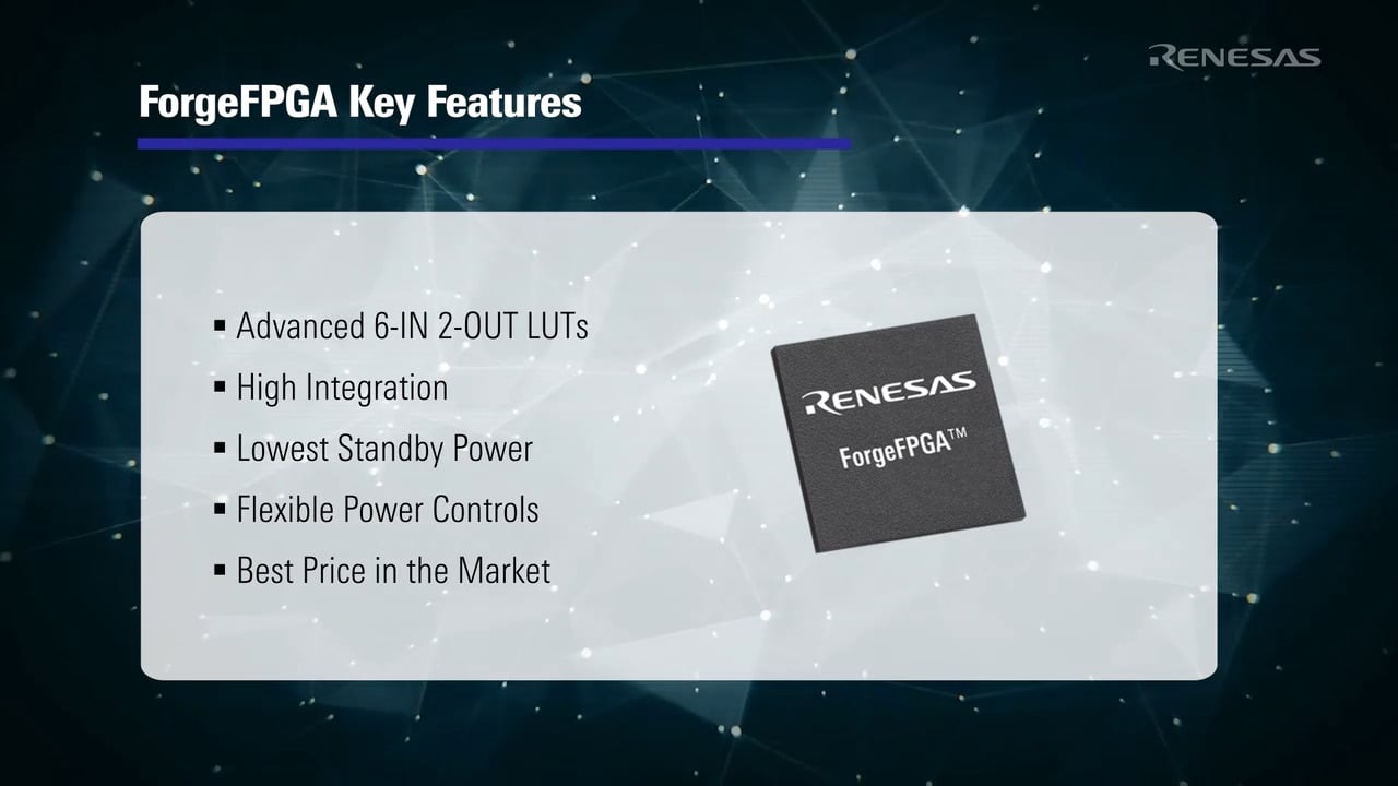
- Ultra-low power consumption for use in even the most demanding wearable and power-constrained applications
- Small package size to allow for tremendous design flexibility
- Advanced 6-input 2-output lookup table (LUT) structure for increased efficiency in high-usage designs
- Low price that opens the low-density FPGA market to customers of all sizes
Parameters
| Attributes | Value |
|---|---|
| Vddc | 1.05 - 1.15 |
| Vddio | 1.71 - 3.465 |
| GPIOs (#) | 19 |
| Look-up Table (LUTs) | 1120 |
| D Flip-flops (DFFs) (#) | 1120 |
| BRAM (kbit) | 32 |
| Distributed Memory (kbit) | 5 |
| Vddio Domains (#) | 1 |
| LVDS Channels (#) | 0 |
| On-chip Oscillator | Yes |
| On-chip Oscillator Freq. | 50MHz |
| PLLs | 1 |
| Configuration Modes | SPI Controller, SPI Target, OTP |
| Memory Type | OTP |
| Temp. Range (°C) | -40 to +85°C |
| Sleep/Reset Mode Current (µA) | 14 |
| Static State Iddc (µA) | 52 |
| Special Features | Sleep Mode |
Package Options
| Pkg. Type | Pkg. Dimensions (mm) | Lead Count (#) | Pitch (mm) |
|---|---|---|---|
| STQFN | 3.0 x 3.0 0.4 pitch | 24 | 0.4 |
Application Block Diagrams
 | Smart Wireless Wall Clock Compact, low-cost clock design with a smooth transition of digits and automatic brightness adjustment. |
Additional Applications
- Sensor data aggregation and pipelining
- Protocol conversion
- Glue logic and edge processing
- Advanced power sequencing
- Consumer electronics
- Data communications equipment
- Notebooks and tablet PCs
Complete Your Design
Explore complementary products to elevate your design
Renesas Boards & Kits
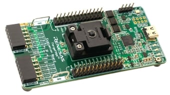
1K LUT ForgeFPGA Evaluation Board
The SLG7EVBFORGE ForgeFPGA evaluation board is a compact, easy-to-use, USB-powered hardware tool that provides SLG47910V 1K lookup table (LUT) ForgeFPGA IC hardware support for design emulation, programming, and real-time testing. The evaluation board is controlled by Renesas' Go Configure™... Read More
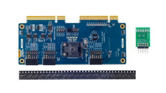
ForgeFPGA SLG47910V Socket Card Kit
The SLG47910V-SKT is a socket card kit for use with the SLG4DVKGOCONF Go Configure Development Board. The SLG47910V-SKT kit includes the ForgeFPGA™ Socket Card #1 (SLG7SC1), 20 samples of SLG47910V, and a Pmod™ LED adapter.
The ForgeFPGA Socket Card #1 is a development board designed for... Read More
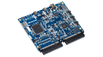
Go Configure Development Board
The Go Configure™ Development Board is a universal development board for Renesas' ForgeFPGA products that supports all features of the Go Configure™ Software Hub. A set of compatible socket cards is available for a quick and easy start to the development process. This board is ideal for rapid... Read More
Support Communities
-
SLG47910 BRAM: Can it handle 100MHz Clocks? Exploring Solutions for Data Buffering
Hi. I´m working a concept study for using a SLG47910. I want to use the BRAM Module to buffer data, but in my system, I have both internal clocks already used and configured with 100MHz (one is 180° shifted). In the datasheet the frequency limit for BRAM is much ...
Nov 24, 2025 -
What is the expected price of the SLG47910 ForgeFPGA?
Anybody has any estimation on the expected price of the SLG47910 ForgeFPGA? e.g. compare to a SLG46826? I would like to know if I should hold my breath. Thanks.
Jan 25, 2024 -
SLG47910 ForgeFPGA IC Availability in 2025
The evaluation board for the SGL47910 is available, but purchasing units of the IC in less than reel qty (100..200 units) seems an impossible task, and I don't want to design something only to find out I'd be required to purchase 5000 units. When is this IC ...
Feb 6, 2025
Knowledge Base
-
Can I use SPI Flash from another vendor?
... read: 0Bh Power-down or deep-sleep: B9h Should exit power-down or deep sleep mode in less than 300us Required Flash memory capacity depends on used device: for SLG47910 it is at least 384kbit; for SLG47912/20/21 it is at least 769kbit. Suitable Products ForgeFPGA™
Mar 25, 2026 -
What drive strength options are available for GPOs?
Last Updated: 03/25/2026 Question: What drive strength options are available for GPOs? Answer: In SLG47910 two drive strength options available: 4/8 mAIn SLG47912, SLG47920, SLG47921 three drive strength options available - 4/8/12 mA Suitable Products ForgeFPGA™
Mar 25, 2026 -
Is it possible to initialize the BRAM block?
Last Updated: 03/25/2026 Question: Is it possible to initialize the BRAM block? Answer: BRAM initialization is not supported on the SLG47910. However, it is supported on the SLG47912, SLG47920, and SLG47921. Suitable Products ForgeFPGA™
Mar 25, 2026

Support Communities


