| Lead Count (#) | 240 |
| Pkg. Type | FCCSP |
| Pkg. Code | AVG240 |
| Pitch (mm) | 0.65 |
| Pkg. Dimensions (mm) | 13.5 x 8.7 x 0.9 |
| Moisture Sensitivity Level (MSL) | 3 |
| Pb (Lead) Free | Yes |
| ECCN (US) | |
| HTS (US) |
| Pkg. Type | FCCSP |
| Lead Count (#) | 240 |
| Carrier Type | Reel |
| Moisture Sensitivity Level (MSL) | 3 |
| Qty. per Reel (#) | 3000 |
| Qty. per Carrier (#) | 0 |
| Pb (Lead) Free | Yes |
| Pb Free Category | e1 SnAgCu |
| Temp. Range (°C) | 0 to 70°C |
| Function | DDR5 Gen 3.0 Server RCD |
| Input Voltage Range (V) | 1.06 - 1.16 |
| Length (mm) | 13.5 |
| MOQ | 3000 |
| Pitch (mm) | 0.65 |
| Pkg. Dimensions (mm) | 13.5 x 8.7 x 0.9 |
| Reel Size (in) | 13 |
| Supply Voltage (V) | 1.06 - 1.16 |
| Tape & Reel | Yes |
| Thickness (mm) | 0.9 |
| Width (mm) | 8.7 |
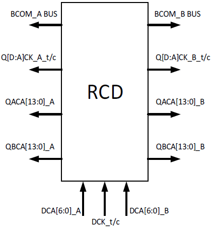
The RG5R364 (Gen 3 RCD) is a registering clock driver used on DDR5 RDIMMs. It supports DDR5 server speeds up to 6400 MT/s. Its primary function is to buffer the Command Address (CA) bus, chip selects, and clock between the host controller and the DRAMs.
The RG5R364 contains two separate channels with some common logic such as clocking, but otherwise operate independently of each other. Each channel has a 7-bit double data rate CA bus input, a single parity input, two chip-select inputs, produces two copies of 14-bit single data rate CA bus outputs and two copies of the chip-select outputs. The RCD has a common clock input and PLL, but produces separate clock outputs to the DRAM channels.