| Pkg. Type: | VFQFPN |
| Pkg. Code: | NDG40 |
| Lead Count (#): | 40 |
| Pkg. Dimensions (mm): | 5.0 x 5.0 x 0.9 |
| Pitch (mm): | 0.4 |
| Moisture Sensitivity Level (MSL) | 3 |
| Pb (Lead) Free | Yes |
| ECCN (US) | EAR99 |
| HTS (US) | 8542.39.0090 |
| Pkg. Type | VFQFPN |
| Lead Count (#) | 40 |
| Carrier Type | Tray |
| Moisture Sensitivity Level (MSL) | 3 |
| Pkg. Dimensions (mm) | 5.0 x 5.0 x 0.9 |
| Qty. per Reel (#) | 0 |
| Diff. Outputs | 8 |
| Input Type | LVDS, LP-HCSL, LVCMOS |
| Outputs (#) | 16 |
| Package Area (mm²) | 25 |
| Qty. per Carrier (#) | 490 |
| Pb (Lead) Free | Yes |
| Pb Free Category | e3 Sn |
| Temp. Range (°C) | -40 to 85°C |
| Price (USD) | 5.09405 |
| Advanced Features | Programmable Clock |
| App Jitter Compliance | PCIe Gen1, PCIe Gen2, PCIe Gen3, PCIe Gen4, PCIe Gen5, PCIe Gen6, PCIe Gen7 |
| Application | Data Center Accelerators, Switches, Routers, Synchronous Ethernet |
| Architecture | Common, SRIS, SRNS |
| C-C Jitter Max P-P (ps) | 50 |
| Channels (#) | 1 |
| Core Voltage (V) | 1.8, 2.5, 3.3 |
| Diff. Inputs | 2 |
| Diff. Output Signaling | LP-HCSL, LVDS, LVPECL, LVCMOS |
| Family Name | VersaClock® 7 |
| Fractional Output Dividers (#) | 3 |
| Function | Generator |
| Input Freq (MHz) | - |
| Inputs (#) | 2 |
| Length (mm) | 5 |
| Longevity | 2040 Apr |
| MOQ | 490 |
| Output Banks (#) | 6 |
| Output Freq Range (MHz) | - |
| Output Impedance | 85, 100 |
| Output Skew (ps) | 30 |
| Output Type | LVDS, LP-HCSL, LVCMOS |
| Output Voltage (V) | 1.8, 2.5, 3.3 |
| Phase Jitter Typ RMS (fs) | 150 |
| Phase Jitter Typ RMS (ps) | 0.15 |
| Pitch (mm) | 0.4 |
| Power Consumption Typ (mW) | 1000 |
| Product Category | VersaClock |
| Prog. Clock | Yes |
| Prog. Interface | OTP, I2C, SPI, SMBUS, EEPROM |
| Published | No |
| Reference Output | No |
| Requires Terms and Conditions | Does not require acceptance of Terms and Conditions |
| Spread Spectrum | Yes |
| Supply Voltage (V) | - , - , - |
| Tape & Reel | No |
| Thickness (mm) | 0.9 |
| Width (mm) | 5 |
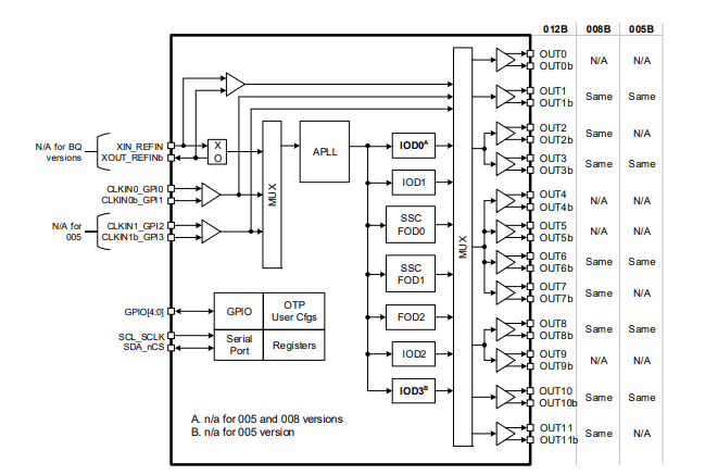
The RC21xxxB (RC21012B and RC21008B) is a member of Renesas's VersaClock® 7 programmable clock generator family. It is intended for high-performance computers, data communications, and industrial applications, designed to be placed immediately adjacent to a PHY, switch, ASIC or FPGA that requires several reference clocks with jitter performance 150fs typical RMS.
Up to 27 configurations reusable across multiple designs may be stored in on-chip One-Time Programmable (OTP) memory or external I2C EEPROM. Redundant input is available for backup and used as a reference clock where needed.