
Features
- LP-HCSL outputs eliminate up to 96 terminated resistors
- PCIe Gen 1–7 compliance
- Drive both source-terminated and double-terminated loads
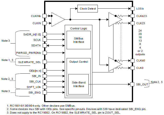
- Selectable output slew rate via SMBus
- Supports 85Ω output impedance
- Open-drain LOS (Loss-Of-Signal) indication output
- Power down tolerance (PDT)
- Flexible startup sequencing (FSS)
- Automatic clock parking (ACP)
- Dedicated OE# pins to control group output
- 4-wire Side-Band interface and device daisy-chaining
- SMBus write protection features with 9 selectable addresses
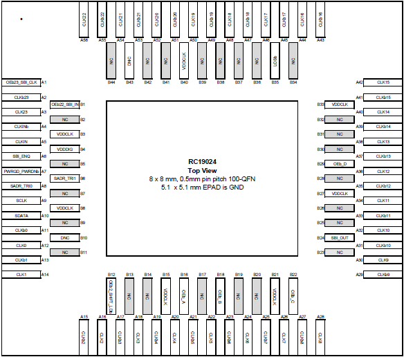
- 8mm × 8mm 100-GQFN package
Description
The RC19024 is a 24-output PCIe Gen7 buffer that is backward compatible with earlier PCIe generations. The RC19024 provides ultra-low additive jitter and reduced in-to-out delay performance for better design margin and incorporates several features for easier and more robust design.
Parameters
| Attributes | Value |
|---|---|
| Diff. Outputs | 24 |
| Diff. Output Signaling | LP-HCSL |
| Output Freq Range (MHz) | 1 - 400 |
| Diff. Inputs | 1 |
| Power Consumption Typ (mW) | 808 |
| Supply Voltage (V) | 3.3 - 3.3 |
| Output Type | LP-HCSL |
| Battery Backup | No |
| Battery Seal | No |
| CPU Supervisory Function POR | No |
| Crystal Frequency Trimming | No |
| Frequency Out Pin | No |
| Inputs (#) | 1 |
| Input Freq (MHz) | 1 - 400 |
| Adjustable Phase | No |
| Noise Floor (dBc/Hz) | -154 |
| Channels (#) | 2 |
| Additive Phase Jitter Typ RMS (fs) | 30 |
| Function | Fanout Buffer |
| Input Type | LVDS, HCSL |
| Output Banks (#) | 1 |
| Core Voltage (V) | 3.3 |
| Output Voltage (V) | 0.8 |
| Product Category | Clock Buffers & Drivers, PCI Express Clocks |
Package Options
| Pkg. Type | Pkg. Dimensions (mm) | Lead Count (#) | Pitch (mm) |
|---|---|---|---|
| VFQFPN | 8.0 x 8.0 x 0.55 | 100 | 0.5 |