
Features
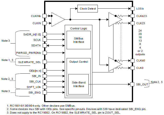
- LP-HCSL outputs eliminate up to 64 terminated resistors
- PCIe Gen 1–7 compliance
- Drive both source-terminated and double-terminated loads
- Selectable output slew rate via pin
- Support both 85Ω and 100Ω output impedance versions
- Open-drain LOS (Loss-Of-Signal) indication output
- Power down tolerance (PDT)
- Flexible startup sequencing (FSS)
- Automatic clock parking (ACP)
- Dedicated OE# pins for each output
- 4-wire Side-Band interface and device daisy-chaining
- SMBus write protection features with 9 selectable addresses
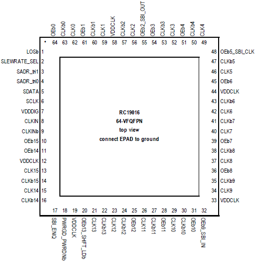
- 9mm x 9mm 64-VFQFPN package
Description
The RC19016 is a 16-output PCIe Gen7 buffer that is backward compatible with earlier PCIe generations. The RC19016 provides ultra-low additive jitter and reduced in-to-out delay performance for better design margin and incorporates several features for easier and more robust design.
Parameters
| Attributes | Value |
|---|---|
| Diff. Outputs | 16 |
| Diff. Output Signaling | LP-HCSL |
| Output Freq Range (MHz) | 1 - 400 |
| Diff. Inputs | 1 |
| Power Consumption Typ (mW) | 498, 508 |
| Supply Voltage (V) | 3.3 - 3.3 |
| Output Type | LP-HCSL |
| Battery Backup | No |
| Battery Seal | No |
| CPU Supervisory Function POR | No |
| Crystal Frequency Trimming | No |
| Frequency Out Pin | No |
| Inputs (#) | 1 |
| Input Freq (MHz) | 1 - 400 |
| Adjustable Phase | No |
| Noise Floor (dBc/Hz) | -154 |
| Channels (#) | 2 |
| Additive Phase Jitter Typ RMS (fs) | 30 |
| Function | Fanout Buffer |
| Input Type | LVDS, HCSL |
| Output Banks (#) | 1 |
| Core Voltage (V) | 3.3 |
| Output Voltage (V) | 0.8 |
| Product Category | Clock Buffers & Drivers, PCI Express Clocks |
Package Options
| Pkg. Type | Pkg. Dimensions (mm) | Lead Count (#) | Pitch (mm) |
|---|---|---|---|
| VFQFPN | 9.0 x 9.0 x 0.9 | 64 | 0.5 |
| Part Number | Status | Samples | Longevity | Stock | Package | Budgetary Price (USD) | Lead Count (#) | Carrier Type | Moisture Sensitivity Level (MSL) | Output Impedance | Power Consumption Typ (mW) | Qty. per Reel (#) | Qty. per Carrier (#) | Pb (Lead) Free | Pb Free Category | Temp. Range (°C) | Country of Assembly | Country of Wafer Fabrication |
|---|---|---|---|---|---|---|---|---|---|---|---|---|---|---|---|---|---|---|
| RC19016A100GN1#BB0 | Active | Available | 2040 Apr | In Stock | VFQFPN | 1ku | $2.15 | 64# | Tray | 3 | 100 | 498mW | 0 | 207# | Yes | e3 Sn | -40 to 105°C | TAIWAN | TAIWAN |
| RC19016A100GN1#KB0 | Active | N/A | 2040 Apr | Out of Stock | VFQFPN | 1ku | $2.15 | 64# | Reel | 3 | 100 | 498mW | 3000# | 0 | Yes | e3 Sn | -40 to 105°C | TAIWAN | TAIWAN |
| RC19016AGN1#BB0 | Active | Available | 2040 Apr | In Stock | VFQFPN | 1ku | $2.15 | 64# | Tray | 3 | 85 | 508mW | 0 | 207# | Yes | e3 Sn | -40 to 105°C | TAIWAN | TAIWAN |
| RC19016AGN1#KB0 | Active | N/A | 2040 Apr | Out of Stock | VFQFPN | 1ku | $2.15 | 64# | Reel | 3 | 85 | 508mW | 3000# | 0 | Yes | e3 Sn | -40 to 105°C | TAIWAN | TAIWAN |
Filters
Applied Filters
- Application NotePDF 2.66 MB R31AN0080EU0102 Rev.1.02 Jun 02, 2026AI-generated Summary: Layout recommendations focus on PCIe Buffer/Mux devices across several families, emphasizing optimal PCB layer stack-up, trace sizing, and signal routing. Key points include using microstrip impedance calculations and tools like Polar Instruments for trace design, following common layout rules such as avoiding right-angle bends, and ensuring proper power supply, clocking, EMI-EMC, and thermal layouts. The document provides detailed guidance on signal integrity, current return paths, crosstalk reduction, and EPAD thermal management to enhance PCIe timing device performance.
- DatasheetRC190xx DatasheetRECOMMENDEDPDF 876 KB R31DS0016EU0129 Rev.1.29 May 11, 2026The RC190xx (RC19024, RC19020, RC19020A072, RC19016, RC19013, RC19008, RC19004, and RC19002) ultra-high performance fanout buffers support PCIe Gen1-7. The devices provide a Loss-Of-Signal (LOS) output for system monitoring and redundancy. The RC190xx also incorporate Power Down Tolerant (PDT) and Flexible Startup Sequencing (FSS) features, easing system design. They can drive both source-terminated and double-terminated loads, operating up to 400MHz. This document describes the main design and operational characteristics for RC190xx devices, including pin information, specifications, applications information, and packaging.
- Application NotePDF 431 KB 7WDXRDKU4E7E-5-59216 Dec 06, 2023
- White PaperPDF 1.35 MB 7WDXRDKU4E7E-6-61930 Aug 05, 2020As PCIe data rates increase and jitter budgets tighten, accurately measuring reference clock jitter becomes more challenging. This paper examines how intrinsic jitter in test setups impacts measurement accuracy and compares results from Phase Noise Analyzers and digital sampling oscilloscopes. It also explores methods to isolate and correct for intrinsic jitter using noiseless PCIe Gen5 clock sources and real-world components such as fan-out buffers and clock generators.
- Application NotePDF 235 KB 7WDXRDKU4E7E-5-58851 Apr 08, 2015
- Application NotePDF 495 KB 7WDXRDKU4E7E-5-57312 May 12, 2014
- Application NotePDF 442 KB 7WDXRDKU4E7E-5-57298 May 08, 2014
- Application NotePDF 160 KB 7WDXRDKU4E7E-5-57287 May 06, 2014
- Application NotePDF 1.99 MB 7WDXRDKU4E7E-5-57242 Mar 01, 2022
- DatasheetRC190xx DatasheetRECOMMENDEDPDF 876 KB R31DS0016EU0129 Rev.1.29 May 11, 2026The RC190xx (RC19024, RC19020, RC19020A072, RC19016, RC19013, RC19008, RC19004, and RC19002) ultra-high performance fanout buffers support PCIe Gen1-7. The devices provide a Loss-Of-Signal (LOS) output for system monitoring and redundancy. The RC190xx also incorporate Power Down Tolerant (PDT) and Flexible Startup Sequencing (FSS) features, easing system design. They can drive both source-terminated and double-terminated loads, operating up to 400MHz. This document describes the main design and operational characteristics for RC190xx devices, including pin information, specifications, applications information, and packaging.
Recommended Documents (1)
- DatasheetRC190xx DatasheetRECOMMENDEDPDF 876 KB R31DS0016EU0129 Rev.1.29 May 11, 2026The RC190xx (RC19024, RC19020, RC19020A072, RC19016, RC19013, RC19008, RC19004, and RC19002) ultra-high performance fanout buffers support PCIe Gen1-7. The devices provide a Loss-Of-Signal (LOS) output for system monitoring and redundancy. The RC190xx also incorporate Power Down Tolerant (PDT) and Flexible Startup Sequencing (FSS) features, easing system design. They can drive both source-terminated and double-terminated loads, operating up to 400MHz. This document describes the main design and operational characteristics for RC190xx devices, including pin information, specifications, applications information, and packaging.
Datasheets (1)
No Results Found.
Make sure all keywords are spelled correctly.
Try fewer, different, or more general terms to vary your search.
If you have filters applied, consider deselecting some to broaden your results.
- Search our extensive knowledgebase, designed to help customers with their FAQs.
- Get help from our expert Renesas technical staff and community on our support forums.
- Application NotePDF 2.66 MB R31AN0080EU0102 Rev.1.02 Jun 02, 2026AI-generated Summary: Layout recommendations focus on PCIe Buffer/Mux devices across several families, emphasizing optimal PCB layer stack-up, trace sizing, and signal routing. Key points include using microstrip impedance calculations and tools like Polar Instruments for trace design, following common layout rules such as avoiding right-angle bends, and ensuring proper power supply, clocking, EMI-EMC, and thermal layouts. The document provides detailed guidance on signal integrity, current return paths, crosstalk reduction, and EPAD thermal management to enhance PCIe timing device performance.
- Application NotePDF 431 KB 7WDXRDKU4E7E-5-59216 Dec 06, 2023
- Application NotePDF 1.99 MB 7WDXRDKU4E7E-5-57242 Mar 01, 2022
- White PaperPDF 1.35 MB 7WDXRDKU4E7E-6-61930 Aug 05, 2020As PCIe data rates increase and jitter budgets tighten, accurately measuring reference clock jitter becomes more challenging. This paper examines how intrinsic jitter in test setups impacts measurement accuracy and compares results from Phase Noise Analyzers and digital sampling oscilloscopes. It also explores methods to isolate and correct for intrinsic jitter using noiseless PCIe Gen5 clock sources and real-world components such as fan-out buffers and clock generators.View More (10)
Application Notes & White Papers (10)
Product Notices (PCN, EOL, etc) (1)
No Results Found.
Make sure all keywords are spelled correctly.
Try fewer, different, or more general terms to vary your search.
If you have filters applied, consider deselecting some to broaden your results.
- Search our extensive knowledgebase, designed to help customers with their FAQs.
- Get help from our expert Renesas technical staff and community on our support forums.
No Results Found.
Make sure all keywords are spelled correctly.
Try fewer, different, or more general terms to vary your search.
If you have filters applied, consider deselecting some to broaden your results.
- Search our extensive knowledgebase, designed to help customers with their FAQs.
- Get help from our expert Renesas technical staff and community on our support forums.
Schematics & Design Files (1)
No Results Found.
Make sure all keywords are spelled correctly.
Try fewer, different, or more general terms to vary your search.
If you have filters applied, consider deselecting some to broaden your results.
- Search our extensive knowledgebase, designed to help customers with their FAQs.
- Get help from our expert Renesas technical staff and community on our support forums.
No Results Found.
Make sure all keywords are spelled correctly.
Try fewer, different, or more general terms to vary your search.
If you have filters applied, consider deselecting some to broaden your results.
- Search our extensive knowledgebase, designed to help customers with their FAQs.
- Get help from our expert Renesas technical staff and community on our support forums.
No Results Found.
Make sure all keywords are spelled correctly.
Try fewer, different, or more general terms to vary your search.
If you have filters applied, consider deselecting some to broaden your results.
- Search our extensive knowledgebase, designed to help customers with their FAQs.
- Get help from our expert Renesas technical staff and community on our support forums.
Marketing Collateral (1)
No Results Found.
Make sure all keywords are spelled correctly.
Try fewer, different, or more general terms to vary your search.
If you have filters applied, consider deselecting some to broaden your results.
- Search our extensive knowledgebase, designed to help customers with their FAQs.
- Get help from our expert Renesas technical staff and community on our support forums.
No Results Found.
Make sure all keywords are spelled correctly.
Try fewer, different, or more general terms to vary your search.
If you have filters applied, consider deselecting some to broaden your results.
- Search our extensive knowledgebase, designed to help customers with their FAQs.
- Get help from our expert Renesas technical staff and community on our support forums.
No Results Found.
Make sure all keywords are spelled correctly.
Try fewer, different, or more general terms to vary your search.
If you have filters applied, consider deselecting some to broaden your results.
- Search our extensive knowledgebase, designed to help customers with their FAQs.
- Get help from our expert Renesas technical staff and community on our support forums.
Filters
Applied Filters
Software & Tools
Filter by Type
Filter by Provider
Sample Code
Filter by Application
Filter by Function
Filter by Compiler
Filter by IDE
Simulation Models
Partner Solutions
No Results Found.
Make sure all keywords are spelled correctly.
Try fewer, different, or more general terms to vary your search.
If you have filters applied, consider deselecting some to broaden your results.
- Search our extensive knowledgebase, designed to help customers with their FAQs.
- Get help from our expert Renesas technical staff and community on our support forums.
Software & Tools (2)
No Results Found.
Make sure all keywords are spelled correctly.
Try fewer, different, or more general terms to vary your search.
If you have filters applied, consider deselecting some to broaden your results.
- Search our extensive knowledgebase, designed to help customers with their FAQs.
- Get help from our expert Renesas technical staff and community on our support forums.
Simulation Models (1)
No Results Found.
Make sure all keywords are spelled correctly.
Try fewer, different, or more general terms to vary your search.
If you have filters applied, consider deselecting some to broaden your results.
- Search our extensive knowledgebase, designed to help customers with their FAQs.
- Get help from our expert Renesas technical staff and community on our support forums.
The RC family consists of PCIe Gen7 clock buffer and multiplexer solutions, providing the industry's smallest and most compact footprint.
Introducing Renesas’ enhanced PCIe clock buffer family. These PCIe Gen5 clock buffers offer fanout and zero-delay operating modes, supporting both legacy systems and the most complex timing trees within a single device. Unlike many existing solutions, whose performance limitations force their use in fanout buffer mode, these clock buffers meet both PCIe Gen5 and prominent CPU-specific phase jitter requirements in all operating modes. The extremely low 50fs rms PCIe Gen5 additive phase jitter enables multi-level cascading within the strict PCIe Gen5 jitter budget. Renesas’ high-performance oscillators and clock generators provide an ideal clock source for the enhanced PCIe clock buffer family.
A detailed overview of IDT's full-featured PCI Express (PCIe) clock and timing solutions. The presentation addresses PCIe Gen 1, Gen 2, Gen 3, and Gen 4 architectures and how IDT's industry-leading solutions provide all the functions, features, and performance required by the application.
Presented by Ron Wade, System Architect at IDT. For more information visit the PCIe clocks page.
The 9ZXL1951D is designed to create clocks for PCI Express Generation 4. This video demonstrates how the reference clock for the 9ZXL1951D does not need to be PCI Express Gen4 compliant. When using the Low Bandwidth mode, the 9ZXL1951D will attenuate jitter so its output clocks still pass PCI Express Gen4, even when the input clock only passes PCI Express Gen3. This is most useful when the clock has spread spectrum modulation because it is very difficult to make a very low noise spreading clock.
A brief overview of how data rates have changed from PCI Express (PCIe) Generation 1, Gen 2, Gen 3, Gen 4 and Gen 5.
Presented by Ron Wade, system architect at IDT.
A brief overview of how clock and timing specifications have changed from PCI Express (PCIe) Generation 1, Gen 2, Gen 3, Gen 4 and Gen 5.
Presented by Ron Wade, system architect at IDT (acquired by Renesas).
A brief overview of the PCI Express common clock (CC) jitter model, and the transfer functions as they relate to the timing PLLs. This model applies to PCI Express (PCIe) Gen 2, Gen 3, Gen 4 and Gen 5. The equations would be slightly different for other PCIe architectures, such as SRIS, SRnS, or data clocked.
Presented by Ron Wade, system architect at IDT (acquired by Renesas). For more information about Renesas's PCIe timing solutions, visit the PCI Express (PCIe) Clocks page.
This video compares PCIe Gen3–7 common clock jitter filters with a typical 12kHz to 20MHz plot to highlight the differences in filtering approaches.

Support Communities


