Features
- Bidirectional buck, boost, and buck-boost operation
- Configurable for 4-switch buck-boost or 2-switch buck operation
- Input voltage range: 3.8V to 23V (no dead zone)
- Output voltage: up to 21V
- Up to 1MHz switching frequency
- Pin programmable soft-start time
- LDO output for VDD and VDDP
- System FAULT status ALERT function
- Input/output internal discharge function
- Active switching for negative voltage transitions
- Pass Through mode in both directions
- Forward and Reverse mode enable pins
- OCP, OVP, UVP, and OTP protection
- Absolute overvoltage protection
- SMBus and auto-increment I2C compatible
- Pb-free (RoHS compliant)
- 32 Ld 4mm x 4mm TQFN package
- UL 2367, IEC 62368-1: File No. E520109

Description
The RAA489800 is a bidirectional, buck-boost voltage regulator that provides buck-boost voltage regulation and protection features. The advanced Renesas R3™ Technology provides high light-load efficiency, fast transient response, and seamless DCM/CCM transitions. The RAA489800 takes input power from a wide range of DC power sources up to 23V (such as conventional AC/DC adapters (ADP), USB PD ports, travel ADP) and safely converts it to a regulated voltage up to 21V.
The RAA489800 can also convert a wide range DC power source connected at its output (system side) to a regulated voltage to its input (ADP side). This bidirectional buck-boost regulation feature makes the RAA489800's application very flexible. In addition to 4-switch buck-boost configuration, it can also support 2-switch Buck mode operation. The RAA489800 includes various system operation functions such as the Forward mode enable pin, Reverse mode enable pin, programmable soft-start time, and adjustable forward and reverse VOUT. It also has forward and reverse power-good indicators. The protection functionalities include OCP, OVP, UVP, and OTP.
The RAA489800 has serial communication through SMBus/I2C that allows programming of many critical parameters to deliver a customized solution. These programming parameters include, but are not limited to: output current limit, input current limit, and output voltage setting.
Parameters
| Attributes | Value |
|---|---|
| Topology [Rail 1] | Buck-Boost |
| Outputs (#) | 1 |
| Input Voltage (Min) (V) | 3.8 |
| Input Voltage (Max) (V) | 23 |
| Output Voltage (Min) (V) | 2 |
| Output Voltage (Max) (V) | 21 |
| Quiescent Current | 120 uA (forward) |
| Switching Frequency Range (Typical) (kHz) | 620 - 1000 |
| SYNCH Capability | No |
| Parallelable | No |
| Bi-direction | Yes |
| Control Type | Hysteretic Mode |
| Temp. Range (°C) | -40 to +105°C, -40 to +125°C |
Package Options
| Pkg. Type | Pkg. Dimensions (mm) | Lead Count (#) | Pitch (mm) |
|---|---|---|---|
| TQFN | 4.0 x 4.0 x 0.70 | 32 | 0.4 |
Application Block Diagrams
 | Universal USB PD Lab Power Supply & Monitor USB PD portable power supply up to 48V, ideal for engineers' mobile and fieldwork needs. |
 | 100W Adjustable Power Supply with USB PD Input Efficient power supply with USB PD input, adjustable output voltage, and current settings. |
Additional Applications
- Tablets
- Ultrabooks
- Power banks
- Mobile devices
- USB-C
Complete Your Design
Explore complementary products to elevate your design
Renesas Boards & Kits

100W USB Type-C DC Input Module
This is a USB-certified reference design for dual-port sourcing ports. This reference design converts a DC input to two USB Type-C® source ports. USB Type-C® source ports support Programmable Power Supply (PPS).
This reference design has two USB Type-C ports, making it a suitable solution for... Read More

100W USB Type-C Input/Output Power Converter
This is the single port reference design that converts USB Type-C® input power to DC output or DC input to USB Type-C® output sourcing power.
The USB Type-C® port is dual role power (DRP) and supports both sink and source modes.
By using a dedicated FW, this board can also function as a USB PD... Read More
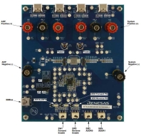
Bidirectional Buck-Boost Voltage Regulator Evaluation Board
The RAA489800 is a bidirectional, buck-boost voltage regulator that provides buck-boost voltage regulation and protection features. The advanced Renesas R3™ Technology provides high light-load efficiency, fast transient response, and seamless DCM/CCM transitions.
The RTKA489800DE0000BU takes... Read More
100W USB Type-C Input Power Converter
This is a USB-certified development kit to convert USB-C input power supplied by a USB Type-C® sourcing device to DC output.
Because there are several losses on the cable, BB-VR, and board, the USB Power Delivery (PD) controller compensates for the USB-C input level to achieve the expected DC... Read More
Test This Board Remotely
Support Communities
-
RAA489800's abnormal operation at Light Load (500mA)
Dear, All. I made a power board using RAA489800 IC. At some case, I found abnormal operation. [Case1] Vin = 12V Vout = 13.5V System Side Load = 500mA ==> periodic oscillation phenomenon , Yellow, Red Color Waveform : Vout [Case2] But, at heavy load(1.5A), It's Okay. I think that this phenomenon ...
Jul 9, 2024 -
Where is the Firmware generation support tool (PDC image generator, PDC-IMGGEN) to compile ROM file for R9A02G011?
I like to use in the next project the R9A02G011 (USB Power Delivery Controller) and RAA489800 (Bidirectional Buck-Boost Voltage Regulator), I understand Renesas has developed the Flash memory image data generator (PDC-IMGGEN), where to find it ?
Apr 25, 2024
Knowledge Base
-
RAA489800 Configuration Support
... 2024 Question: Which configuration does RAA489800 Support? Answer: In addition to 4-switch buck-boost configuration, it can also support 2-switch Buck mode operation. RAA489800 is voltage regulator but if you are looking for Buck-Boost Narrow VDC Battery Charger kindly check RAA489108/RAA489118 Suitable Products RAA489800 RAA489108 ...
Nov 7, 2024

Support Communities


