
Features
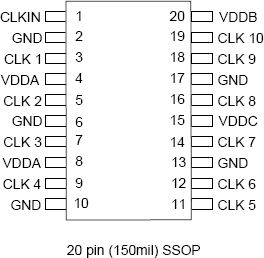
- Packaged in 20-pin QSOP/SSOP
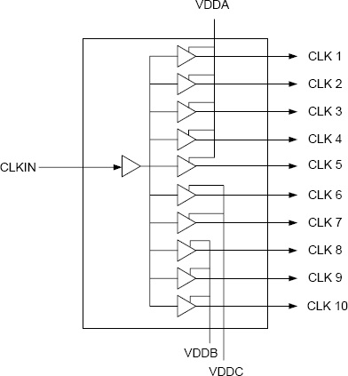
- Split 1:10 fanout Buffer
- Maximum skew between outputs of different packages 0.75 ns
- Max propagation delay of 3.8 ns
- Operating voltage of 1.5 V to 2.5 V on Bank A
- Operating voltage of 1.5 V to 2.5 V on Banks B and C
- Advanced, low power, CMOS process
- Industrial temperature range -40° C to +85° C
- 3.3 V tolerant input when VDDA=2.5 V
- Pb (lead) free packaging
Description
The ICSLV810 is a low skew 1.5 V to 2.5 V, 1:10 fanout buffer. This device is specifically designed for data communications clock management. The large fanout from a single input line reduces loading on the input clock. The TTL level outputs reduce noise levels on the part. Typical applications are clock and signal distribution.