
Features
- Compliant with Intel DB1900G
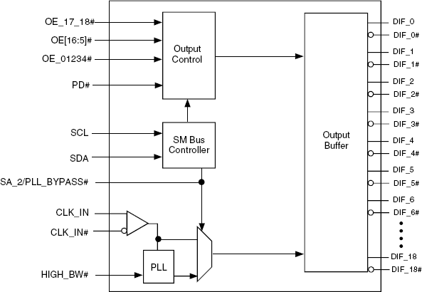
- DIF Clock Support 19 differential clock output pairs @ 0.7 V 150 ps skew performance across all outputs
- OE pin Control of All Outputs
- 3.3 V Operation
- Gear Ratio supporting generation of clocks at a different frequency ratioed from the input.
- Split outputs supporting options of 2 outputs @1:1 and remaining 17 pairs at an alternate gear
- Pin level OE control of individual outputs
- Multiple output frequency options up to 400Mhz as a gear ratio of input clocks of 100-400Mhz
- Output is HCSL compatible
- SMBus Programmable configurations
- PLL Bypass Configurable
- SMBus address configurable to allow multiple buffer control in a single control network
- Programmable Bandwidth
- Glitchfree transition between frequency states
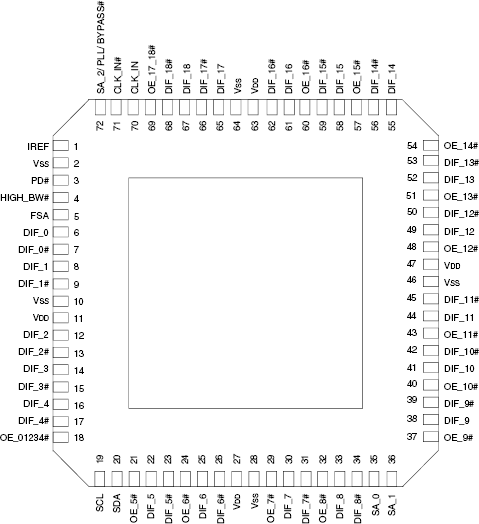
- Available in 72-pin VFQPFN package
Description
The CV145 differential buffer complies with Intel DB1900G , and is designed to work in conjunction with the main clock of CK409, CK410/CK410M and CK410B etc., PLL is off in bypass mode and no clock detect.