
Features
- 1.8V/2.5V/3.3V flexible power rails
- Typical 150fs RMS 12kHz - 20MHz phase jitter
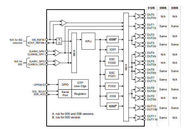
- 5/8/12 outputs with integrated crystal options
- 1kHz to 650MHz LVDS/LP-HCSL outputs
- 1kHz to 200MHz LVCMOS outputs
- Programmable hardware configuration select-pins
- PCIe Gen 5/6/7 ready
- Space saving packages 4mm x 4mm, 5mm x 5mm, 6mm x 6mm
- Integrated crystal option for space saving and BOM optimization


Description
The RC21xxxB (RC21012B and RC21008B) is a member of Renesas's VersaClock® 7 programmable clock generator family. It is intended for high-performance computers, data communications, and industrial applications, designed to be placed immediately adjacent to a PHY, switch, ASIC or FPGA that requires several reference clocks with jitter performance 150fs typical RMS.
Up to 27 configurations reusable across multiple designs may be stored in on-chip One-Time Programmable (OTP) memory or external I2C EEPROM. Redundant input is available for backup and used as a reference clock where needed.
Parameters
| Attributes | Value |
|---|---|
| Diff. Outputs | 5, 8, 12 |
| App Jitter Compliance | PCIe Gen1, PCIe Gen2, PCIe Gen3, PCIe Gen4, PCIe Gen5, PCIe Gen6, PCIe Gen7 |
| Outputs (#) | 16, 24 |
| Output Type | LVDS, LP-HCSL, LVCMOS |
| Output Freq Range (MHz) | 0.001 - 650 |
| Input Freq (MHz) | 1 - 650 |
| Inputs (#) | 2 |
| Input Type | LVDS, LP-HCSL, LVCMOS |
| Output Banks (#) | 6 |
| Core Voltage (V) | 1.8V, 2.5V, 3.3V |
| Output Voltage (V) | 1.8V, 2.5V, 3.3V |
| Product Category | VersaClock, Ultra-Low Jitter Clocks (<300 fs RMS), PCI Express Clocks, Programmable Clocks |
Application Block Diagrams
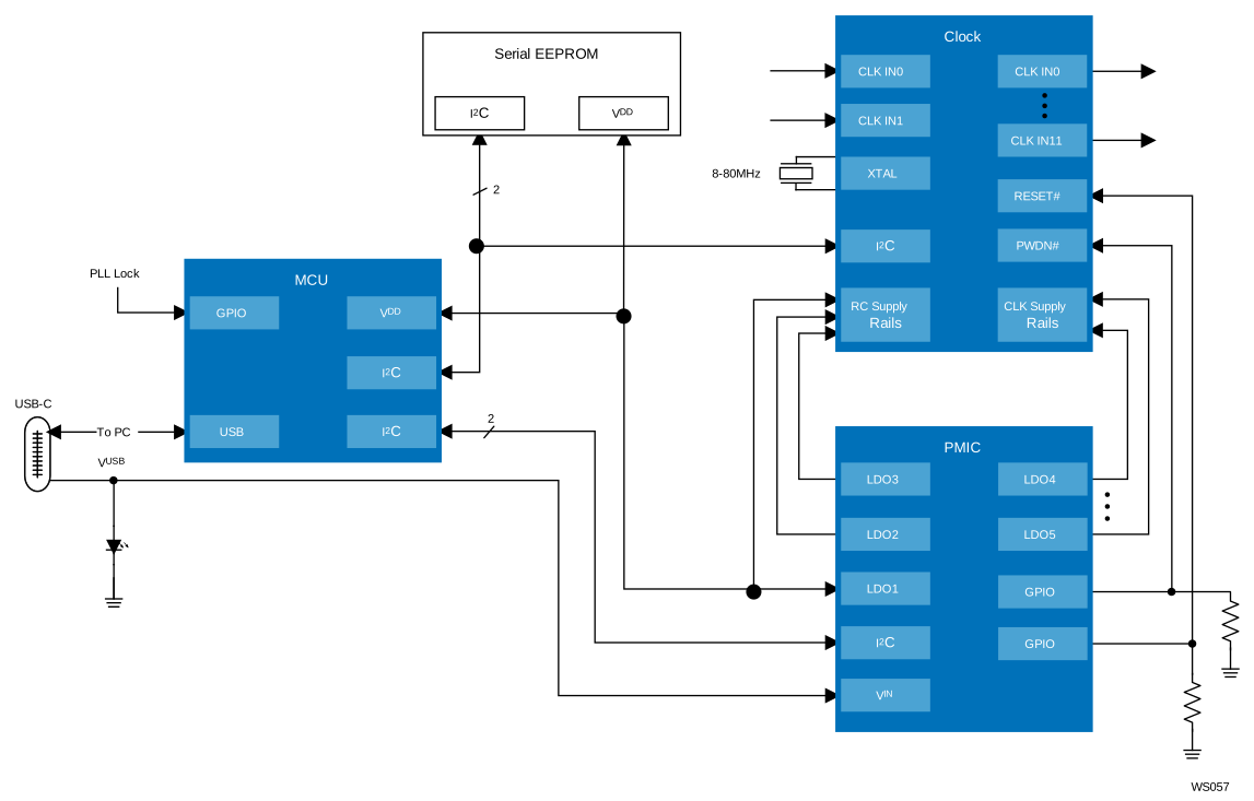 | Reconfigurable High-Performance Clocking System A reconfigurable clocking system enables precise synchronization, real-time adaptability, and design reuse. |
Additional Applications
- High-performance computing
- Datacenter accelerators
- Switches/Routers
- Synchronous Ethernet
- Industrial
Complete Your Design
Explore complementary products to elevate your design
Renesas Boards & Kits

Evaluation Kit for VersaClock 7 Programmable Clock
The RC21008A Evaluation Board (EVB) is designed to support users evaluating the RC21008A using clock generation in synthesizer mode for PCIe Gen 1-6 compliance. When the EVB is connected via USB to the user’s computer running Renesas Integrated Circuit Toolbox (RICBox™) Software, the RC21008 can... Read More
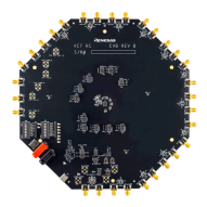
Evaluation Kit for VersaClock 7 Programmable Clock
The RC21012A Evaluation Board (EVB) is designed to support users evaluating the RC21012A using clock generation in synthesizer mode for PCIe Gen 1-6 compliance. When the EVB is connected via USB to the user’s computer running Renesas Integrated Circuit Toolbox (RICBox™) Software, the RC21012A... Read More
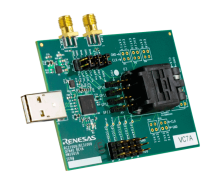
Programming Boards for VersaClock 7 Programmable Clock
The VersaClock® 7 programmer board is made to ease the programming of RC21008 and RC31008 blank devices. With the onboard USB interface, RICBox™ Graphical User Interface (GUI) can be used to communicate with the blank device in the socket for configuration and programming.

Programming Boards for VersaClock 7 Programmable Clock
The VersaClock® 7 programmer board is made to ease the programming of RC21012 and RC31012 blank devices. With the on-board USB interface, RICBox™ Graphical User Interface (GUI) can be used to communicate with the blank device in the socket for configuration and programming.
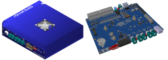
Vehicle Computer Generation 4
The VC4 is based on a complete Renesas chipset. The centerpiece is the R-Car S4 with 8x Cortex®A55 cores, 1x Cortex® R52 core 2x RH850 G4MH delivering up to 27K DMIPS application performance and up to 5.3K DMIPS lock step real-time performance. It incorporates an 8MB SRAM to execute code on the... Read More
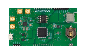
Renesas Timing Product Demo Kit
RCTIMING-DEMO is a Renesas products combination kit. The kit includes a Renesas RL78 MCU, DA14531MOD, Linear Regulators (LDO), RTC (1338-31DVG) and programmable clock generator VersaClock 7 (VC7) to implement a demo kit to support programming clock generator through laptop or smartphone and... Read More
