Features
- LP-HCSL outputs; save 10 resistors compared to standard HCSL outputs
- 35 mW typical power consumption; minimal power consumption
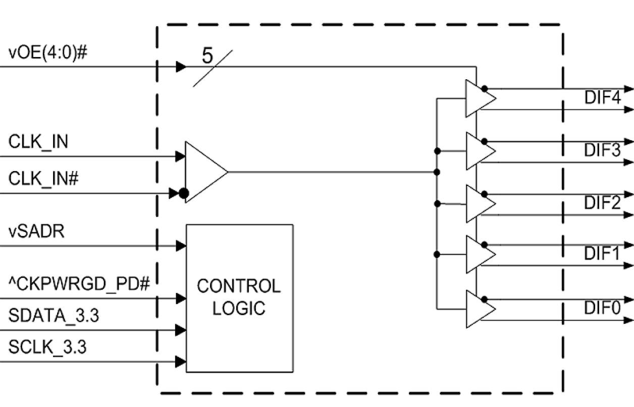
- OE# pin for each output; support DIF power management
- HCSL differential input; can be driven by common clock sources
- Spread spectrum tolerant; allows reduction of EMI
- Programmable slew rate for each output; allows tuning for various line lengths
- Programmable output amplitude; allows tuning for various application environments
- 1 MHz to 167 MHz operating frequency
- 3.3 V tolerant SMBus interface works with legacy controllers
- Selectable SMBus addresses; multiple devices can easily share an SMBus segment
- Device contains default configuration; SMBus interface not required for device operation
- Space-saving 5x5 mm 32-pin VFQFPN; minimal board space
Description
The 9DBU0531 is a member of IDT's 1.5 V Ultra-Low-Power (ULP) PCIe family. The device has 5 output enables for clock management, and 3 selectable SMBus addresses.
Parameters
| Attributes | Value |
|---|---|
| Temp. Range (°C) | -40 to 85°C, 0 to 70°C |
Package Options
| Pkg. Type | Pkg. Dimensions (mm) | Lead Count (#) | Pitch (mm) |
|---|---|---|---|
| VFQFPN | 5.0 x 5.0 x 0.9 | 32 | 0.5 |
Applied Filters:
Filters
Software & Tools
Sample Code
Simulation Models
A detailed overview of IDT's full-featured PCI Express (PCIe) clock and timing solutions. The presentation addresses PCIe Gen 1, Gen 2, Gen 3, and Gen 4 architectures and how IDT's industry-leading solutions provide all the functions, features, and performance required by the application.
Presented by Ron Wade, System Architect at IDT. For more information visit the PCIe clocks page.
This is the first video in our PCIe series. In this video, we define PCIe architectures, focusing on common and separate clock architectures. Watch the rest of the video series below where Ron will cover the impact of different timing architectures.
In this episode, Ron Wade from IDT (acquired by Renesas) explains PCIe common clocking and its impact on timing solutions. Learn about using a single clock source, fan-out buffers, and the considerations for spread spectrum and non-spread spectrum clocking in PCIe systems.
In this video, we explore PCIe with separate reference clocks and the effects of clock selection. Learn how separate reference clocks work and their impact on system performance and stability.
This video provides a high-level overview of Separate Reference Clock with Independent Spread (SRIS) architectures for PCI Express systems, additional performance requirements that this clocking architecture imposes on the reference clocks, and some system implications encountered trying to implement the architecture.
IDT (acquired by Renesas) engineer provides a brief tutorial describing the main differences between standard HCSL and low-power HCSL (LP-HCSL).
Presented by Ron Wade, PCI Express timing expert.
Related Resources
An overview of IDT's full-featured PCI Express (PCIe) clock zero-delay buffers and fanout buffers addressing PCIe Gen 1, Gen 2, Gen 3, and Gen 4.
Presented by Ron Wade, System Architect at IDT.
An overview of PCI Express applications and how IDT's industry-leading portfolio of PCIe clock products addresses the requirements. The video briefly discusses PCIe riser cards, embedded SOC, and PCIe storage (NVME) examples.
Presented by Ron Wade, System Architect at IDT.
A brief overview of how data rates have changed from PCI Express (PCIe) Generation 1, Gen 2, Gen 3, Gen 4 and Gen 5.
Presented by Ron Wade, system architect at IDT. For more information about IDT's PCIe timing solutions, visit the PCI Express (PCIe) Clocks page.
A brief overview of how clock and timing specifications have changed from PCI Express (PCIe) Generation 1, Gen 2, Gen 3, Gen 4 and Gen 5.
Presented by Ron Wade, system architect at IDT (acquired by Renesas). For more information, visit Renesas's PCIe Timing Solutions page.
A brief overview of the PCI Express common clock (CC) jitter model, and the transfer functions as they relate to the timing PLLs. This model applies to PCI Express (PCIe) Gen 2, Gen 3, Gen 4 and Gen 5. The equations would be slightly different for other PCIe architectures, such as SRIS, SRnS, or data clocked.
Presented by Ron Wade, system architect at IDT (acquired by Renesas). For more information about Renesas's PCIe timing solutions, visit the PCI Express (PCIe) Clocks page.