
Features
- 1.8V operation; reduced power consumption
- OE# pins; support DIF power management
- LP-HCSL differential clock outputs; reduced power and board space
- Programmable slew rate for each output; allows tuning for various line lengths
- Programmable output amplitude; allows tuning for various application environments
- DIF outputs are blocked until PLL is locked; clean system start-up
- Selectable 0%, -0.25%, or -0.5% spread on DIF outputs; reduces EMI
- External 25MHz crystal; supports tight ppm with 0ppm synthesis error
- Configuration can be accomplished with strapping pins; SMBus interface is not required for device control
- 3.3V tolerant SMBus interface works with legacy controllers
- Space-saving 5mm x 5mm 32-VFQFPN; minimal board space
- Selectable SMBus addresses; multiple devices can easily share an SMBus segment
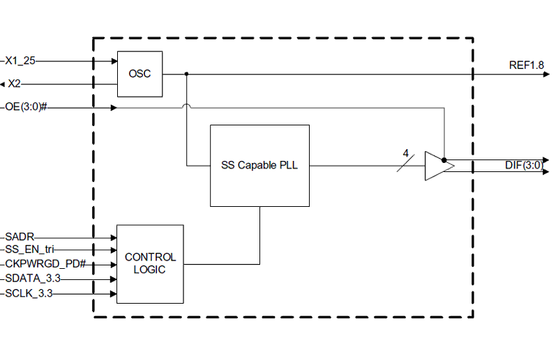
Description
The 9FGV0431 is a 4-output very-low power clock generator for PCIe Gen 1–4 applications. The device has four output enables for clock management and supports two different spread spectrum levels in addition to spread off.
Parameters
| Attributes | Value |
|---|---|
| Diff. Outputs | 4 |
| App Jitter Compliance | PCIe Gen1, PCIe Gen2, PCIe Gen3, PCIe Gen4 |
| Outputs (#) | 5 |
| Output Type | LP-HCSL, LVCMOS |
| Output Freq Range (MHz) | 25 - 25, 100 - 100 |
| Input Freq (MHz) | 25 - 25 |
| Inputs (#) | 1 |
| Input Type | Crystal, LVCMOS |
| Core Voltage (V) | 1.8 |
| Output Voltage (V) | 0.8V, 1.8V |
| Product Category | PCI Express Clocks |
Package Options
| Pkg. Type | Pkg. Dimensions (mm) | Lead Count (#) | Pitch (mm) |
|---|---|---|---|
| VFQFPN | 5.0 x 5.0 x 0.9 | 32 | 0.5 |
Applications
- Riser cards
- Storage
- Networking
- JBOD
- Communications
- Access points