
Features
- Integrated terminations; save 32 resistors compared to standard HCSL outputs
- LP-HCSL outputs; support separate VDDIO rail and 130mW typical power consumption
- 8 OE# pins; hardware control of each output
- 25MHz crystal input; exact synthesis
- 100MHz operation; supports PCIe and SATA applications
- VDDIO; allows outputs to run from lower voltage rail to save power
- OE# pins have 1.5V high input threshold; direct interface to 1.8V to 3.3V systems
- < 130mW power consumption (typical)
- Cycle-to-Cycle jitter < 50ps
- Output-to-Output skew < 100ps
- PCIe Gen 2 phase jitter < 3.0ps RMS
- PCIe Gen 3 phase jitter < 1.0ps RMS
- PCIe Gen 3 SRnS clock phase jitter < 0.7ps RMS

Description
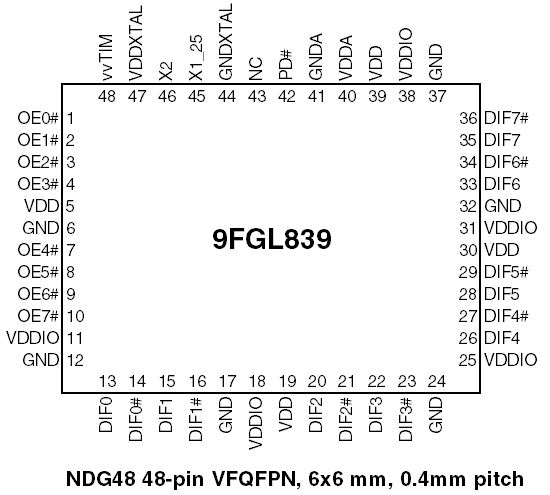
The 9FGL839 is an 8-output differential synthesizer for PCI Express Gen 1, Gen 2, and Gen 3 applications. It has integrated terminations providing direct connection to 100Ω transmission lines and saving 32 resistors compared to standard HCSL outputs. The 9FGL839 supports common, data, and Separate Reference no-Spread (SRnS) PCIe clock architectures.