
Features
- LP-HCSL outputs save 32 resistors; minimal board space and BOM cost
- 62mW typical power consumption in PLL mode; eliminates thermal concerns
- Spread Spectrum (SS) compatible; allows use of SS for EMI reduction
- OE# pins: support DIF power management
- HCSL compatible differential input: can be driven by common clock sources
- Programmable slew rate for each output: allows tuning for various line lengths
- Programmable output amplitude: allows tuning for various application environments
- Pin/Software selectable PLL bandwidth and PLL bypass: minimize phase jitter for each application
- Outputs blocked until PLL is locked: clean system start-up
- Software selectable 50MHz or 125MHz PLL operation: useful for Ethernet applications
- Configuration can be accomplished with strapping pins: SMBus interface not required for device control
- 3.3V tolerant SMBus interface works with legacy controllers
- Space-saving 6mm x 6mm 48-VFQFPN: minimal board space
- Selectable SMBus addresses; multiple devices can easily share an SMBus segment
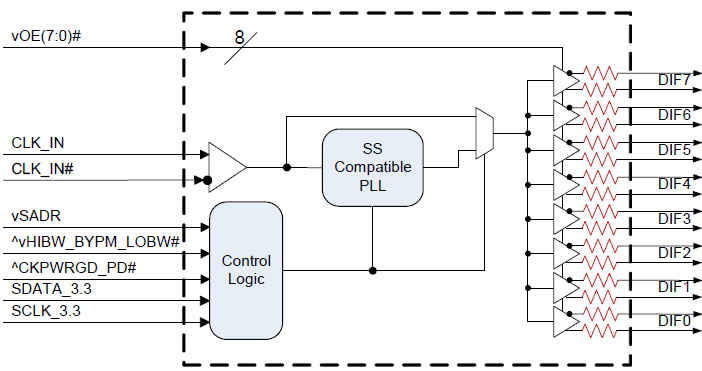
Description
The 9DBV0841 1.8V PCIe Gen 1-3 zero-delay/fanout clock buffer has integrated output terminations providing Zo = 100Ω for direct connection for 100Ω transmission lines. The device has eight output enables for clock management and three selectable SMBus addresses.
Parameters
| Attributes | Value |
|---|---|
| Diff. Outputs | 8 |
| Diff. Output Signaling | LP-HCSL |
| Output Freq Range (MHz) | 1 - 200, 30 - 137.5 |
| Diff. Inputs | 1 |
| Diff. Input Signaling | HCSL |
| Accepts Spread Spec Input | Yes |
| Power Consumption Typ (mW) | 62 |
| Supply Voltage (V) | 1.8 - 1.8 |
| Output Type | LP-HCSL |
| Diff. Termination Resistors | 0 |
| Package Area (mm²) | 36 |
| Battery Backup | No |
| Battery Seal | No |
| CPU Supervisory Function POR | No |
| Crystal Frequency Trimming | No |
| Frequency Out Pin | No |
| Inputs (#) | 1 |
| Input Freq (MHz) | 30 - 175 |
| Divider Value | 1 |
| Additive Phase Jitter Typ RMS (fs) | 250 |
| Function | Zero Delay Buffer |
| Input Type | HCSL |
| Output Banks (#) | 1 |
| Core Voltage (V) | 1.8 |
| Output Voltage (V) | 0.8 |
| Product Category | PCI Express Clocks |
Package Options
| Pkg. Type | Pkg. Dimensions (mm) | Lead Count (#) | Pitch (mm) |
|---|---|---|---|
| VFQFPN | 6.0 x 6.0 x 0.9 | 48 | 0.4 |
Applications
- SSD
- microServers
- WLAN access points