Features
- Compliant with the requirements outlined in Telcordia GR-253-CORE (SONET) and ITU-T G.813/G.8262 (SDH/SONET and SyncE) when paired with a Synchronous Equipment Timing Source (SETS ) device
- Generates up to 4 LVPECL/LVDS/HCSL or 16 LVCMOS output clocks ranging from 8kHz up to 1.0GHz (diff), 8kHz to 250MHz (LVCMOS), that meet jitter limits for 10G up to 25G Ethernet applications
- 0.2ps RMS (including spurs), 12kHz to 20MHz
- Accepts up to two LVPECL, LVDS, LVHSTL, HCSL, or LVCMOS input clocks ranging from 8kHz up to 875MHz
- Auto and manual input clock selection with hitless switching
- Clock input monitoring, including support for gapped clocks
- Phase-Slope Limiting and Fully Hitless Switching options to control output phase transients
- Operates from a 25MHz to 50MHz crystal
- Register programmable through I²C or via external I²C EEPROM
- 8T49N240-991 “Boot from EEPROM”
- 8T49N240-994 “powers up disabled”
- Supported by Renesas' Timing Commander™ software


Description
The 8T49N240 FemtoClock™ NG Universal Frequency Translator (UFT) has one fractional-feedback PLL that can be used as a frequency translator with jitter attenuation or a frequency synthesizer. It is equipped with three integer and one fractional output dividers, allowing the generation of up to two different output frequencies, ranging from 8kHz to 1GHz. Output frequencies can be completely independent of the input frequencies, two of these frequencies can be completely independent of each other and the other two will be integer-related to one of the other two frequencies. The four outputs may select among LVPECL, LVDS, HCSL, or LVCMOS output levels.
The 8T49N240 is ideal for use in a wide range of equipment, including 10G/40G/100G SONET/SDH and Ethernet network line cards, wireless base station baseband units, broadcast video, carrier Ethernet switches, OTN, or in test and measurement applications. For example, the 8T49N240 can be used in GbE/10GbE/100GbE Synchronous Ethernet line card applications to preserve the G.8262 compliance from the Synchronous Equipment Timing Source (SETS) on the timing card. The 8T49N240 provides a 200fs (typical, 12kHz to 20MHz) RMS jitter performance that provides users with additional margin in their designs.
Renesas’ third-generation Universal Frequency Translator family also includes the 8T49N241 (2-in/1-PLL/4-out), 8T49N242 (2-in/1-PLL/4-out), the 8T49N285 (2-in/1-PLL/8-out), the 8T49N286 (4-in/2-PLL/8-out) and the 8T49N287 (2-in/2-PLL/8-out). These devices are complemented by the 82P33714 and 82P33731 Synchronous Equipment Timing Source for Synchronous Ethernet (SyncE) and 10G to 40G SyncE, respectively.
To see other devices in this product family, visit the Universal Frequency Translators page.
Parameters
| Attributes | Value |
|---|---|
| Inputs (#) | 2 |
| Input Type | LVCMOS, HCSL, LVHSTL, LVDS, LVPECL, LVTTL |
| Product Category | FemtoClock NG, IEEE 1588, Low Jitter Clocks (<700 fs RMS), Jitter Attenuators, Network Synchronization, PDH and SONET/SDH Clocks, Programmable Clocks, Universal Frequency Translators, FemtoClock NG, Low Jitter Clocks (<700 fs RMS), IEEE 1588, Low Jitter Clocks (<700 fs RMS), Jitter Attenuators, Network Synchronization, PDH and SONET/SDH Clocks, Programmable Clocks, Universal Frequency Translators |
| Diff. Outputs | 4 |
| Output Type | LVCMOS, LVDS, LVPECL, HCSL |
| Output Voltage (V) | 2.5V, 3.3V, 1.8V |
| Input Freq (MHz) | 0.008 - 875 |
| Phase Jitter Typ RMS (ps) | 0.2 |
| Output Freq Range (MHz) | 0.008 - 1000 |
| Fractional Output Dividers (#) | 3 |
| Core Voltage (V) | 2.5V, 3.3V |
| Output Banks (#) | 4 |
| Loop Bandwidth Range (Hz) | 0.2 - 6400 |
| Xtal Freq (KHz) | 10000 - 50000 |
| Advanced Features | Programmable Hitless Reference Switching, Fractional-N PLL, OTP, External Feedback |
Package Options
| Pkg. Type | Pkg. Dimensions (mm) | Lead Count (#) | Pitch (mm) |
|---|---|---|---|
| VFQFPN | 6.0 x 6.0 x 0.9 | 40 | 0.5 |
Renesas Boards & Kits
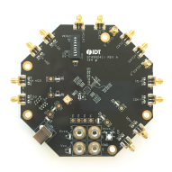
Evaluation Kit for 8T49N240
The 8T49N240-EVK is designed to help the customer evaluate the 8T49N240 Universal Frequency Translator (UFT 3G). When the board is connected to a PC running Timing Commander software™ through USB, the device can be configured and programmed through a graphical interface or through register... Read More
Support Communities
-
External PLL capacitors on the 8T49N240
Hello, The datasheet for the 8T49N240 says that "The 8T49N240 uses two external capacitors of fixed value to support its loop bandwidth" - these being the capacitors between the CAP1/CAP2 pins and CAP_REF, however it does not provide any guidance on how to choose the values of these ...
Mar 26, 2026 -
Clarification on VCCA Pin Grouping and Filtering – 8T49N242
Hello, I am currently implementing the 8T49N242 (3.3 V supply, Q0 configured as ~400 MHz LVDS output) and would like clarification regarding the recommended VCCA supply topology. In the datasheet, pins 1, 30, and 39 are described as PLL supply pins. However, in the Renesas design checklist (Excel document ...
Feb 20, 2026

Support Communities


