
Features
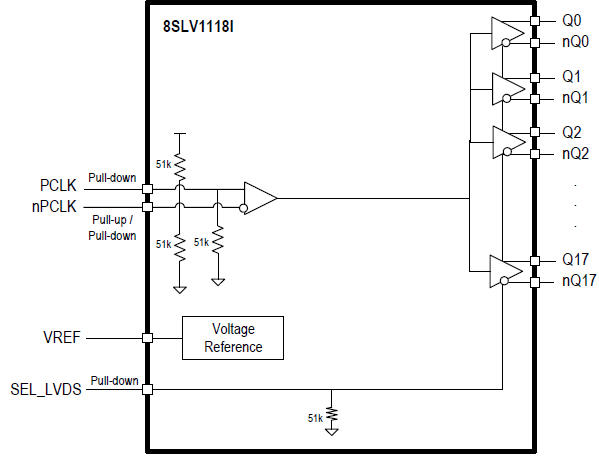
- 1:18, low skew, low additive jitter LVPECL/LVDS fanout buffer
- Low power consumption
- Differential PCLK, nPCLK clock pair accepts the following differential/single-ended input levels: LVDS, LVPECL, and LVCMOS
- Maximum input clock frequency: 2GHz
- Propagation delay: 290ps (typical)
- Output skew: 40ps (typical)
- Low additive phase jitter, RMS: 39fs (typical)
- Integration range: 12kHz–20MHz (fREF = 156.25MHz, VPP = 1V, VDD = 3.3V)
- Full 2.5V and 3.3V supply voltage modes
- Device current consumption:
- 180mA (typical) IEE for LVPECL output mode
- 400mA (typical) IDD for LVDS output mode
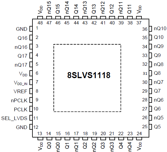
- 48-VFQFN, lead-free (RoHS 6) packaging
- Transistor count: 1762
- -40°C to +85°C ambient operating temperature
- Supports case temperature up to 105°C
Description
The 8SLVS1118 is a high-performance, low-power, differential 1:18 output fanout buffer. This highly versatile device is designed for the fanout of high-frequency, very low additive phase-noise clock and data signals. Guaranteed output-to-output and part-to-part skew characteristics make the 8SLVS1118 ideal for clock distribution applications that demand well-defined performance and repeatability. The device is characterized to operate from a 2.5V or 3.3V power supply. The integrated bias voltage references enable easy interfacing AC-coupled signals to the device inputs.
Parameters
| Attributes | Value |
|---|---|
| Temp. Range (°C) | -40 to 85°C |
| Product Category | Clock Buffers & Drivers, RF Buffers |
Package Options
| Pkg. Type | Pkg. Dimensions (mm) | Lead Count (#) | Pitch (mm) |
|---|---|---|---|
| VFQFPN | 7.0 x 7.0 x 0.9 | 48 | 0.5 |