
Features
- Four differential LVDS output pairs
- One single-ended LVCMOS/LVTTL input
- CLK can accept the following input levels: LVCMOS, LVTTL
- Maximum output frequency: 250MHz
- Translates single-ended input signals to LVDS levels
- Additive phase jitter, RMS: 0.16ps (typical)
- Output skew: 72ps (maximum)
- Part-to-part skew: 350ps (maximum)
- Propagation delay: 1.75ns (maximum)
- 3.3V operating supply
- -40°C to 85°C ambient operating temperature
- Available in lead-free (RoHS 6) package
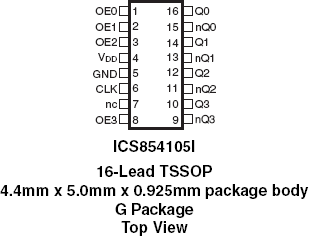
854105I - Pinout
Description
The 854105I is a low skew, high performance 1-to-4 LVCMOS/LVTTL-to-LVDS Clock Fanout Buffer. Utilizing Low Voltage Differential Signaling (LVDS), the 854105I provides a low power, low noise solution for distributing clock signals over controlled impedances of 100?. The 854105I accepts an LVCMOS/LVTTL input level and translates it to LVDS output levels. Guaranteed output and part-to-part skew characteristics make the 854105I ideal for those applications demanding well defined performance and repeatability.

Support Communities
Get quick technical support online from Renesas Engineering Community technical staff.

Knowledge Base
Browse our knowledge base for helpful articles, FAQs, and other useful resources.

