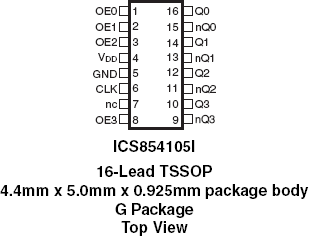
Package Information
| Lead Count (#) | 16 |
| Pkg. Code | PGG16 |
| Pitch (mm) | 0.65 |
| Pkg. Type | TSSOP |
| Pkg. Dimensions (mm) | 5.0 x 4.4 x 1.0 |
Environmental & Export Classifications
| Moisture Sensitivity Level (MSL) | 1 |
| Pb (Lead) Free | Yes |
| ECCN (US) | NLR |
| HTS (US) | 8542390001 |
Product Attributes
| Lead Count (#) | 16 |
| Carrier Type | Reel |
| Moisture Sensitivity Level (MSL) | 1 |
| Qty. per Reel (#) | 2500 |
| Qty. per Carrier (#) | 0 |
| Pb (Lead) Free | Yes |
| Pb Free Category | e3 Sn |
| Temp. Range | -40 to +85°C |
| Additive Phase Jitter Typ RMS (fs) | 160 |
| Additive Phase Jitter Typ RMS (ps) | 0.16 |
| Core Voltage (V) | 3.3 |
| Function | Buffer |
| Input Freq (MHz) | 0 - 250 |
| Input Type | LVCMOS |
| Inputs (#) | 1 |
| Length (mm) | 5 |
| MOQ | 2500 |
| Output Banks (#) | 1 |
| Output Freq Range (MHz) | 0 - 250 |
| Output Skew (ps) | 72 |
| Output Type | LVDS |
| Output Voltage (V) | 3.3 |
| Outputs (#) | 4 |
| Package Area (mm²) | 22.0 |
| Pitch (mm) | 0.65 |
| Pkg. Dimensions (mm) | 5.0 x 4.4 x 1.0 |
| Pkg. Type | TSSOP |
| Reel Size (in) | 13 |
| Requires Terms and Conditions | Does not require acceptance of Terms and Conditions |
| Tape & Reel | Yes |
| Thickness (mm) | 1 |
| Width (mm) | 4.4 |
Resources for 854105I
Description
The 854105I is a low skew, high performance 1-to-4 LVCMOS/LVTTL-to-LVDS Clock Fanout Buffer. Utilizing Low Voltage Differential Signaling (LVDS), the 854105I provides a low power, low noise solution for distributing clock signals over controlled impedances of 100?. The 854105I accepts an LVCMOS/LVTTL input level and translates it to LVDS output levels. Guaranteed output and part-to-part skew characteristics make the 854105I ideal for those applications demanding well defined performance and repeatability.
