
Features
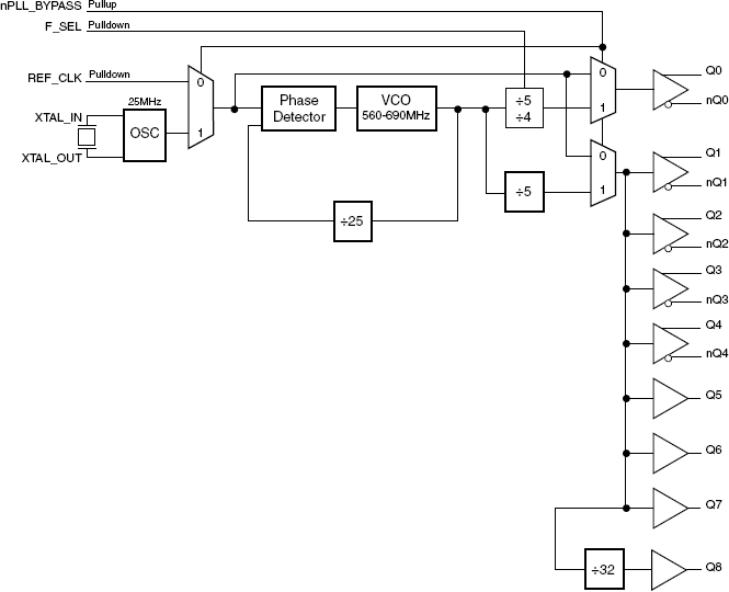
- One differential LVDS output at 156.25MHz or 125MHz Four differential LVDS outputs at 125MHz Three LVCMOS/LVTTL single-ended outputs at 125MHz One LVCMOS/LVTTL single-ended output at 3.90625MHz
- Selectable crystal oscillator interface or LVCMOS/LVTTL single-ended input and PLL bypass from a single select pin
- VCO range: 560MHz - 690MHz
- RMS phase jitter @ 125MHz, using a 25MHz crystal (1.875MHz - 20MHz): 0.45ps (typical), LVDS outputs
- RMS phase jitter @ 156.25MHz, using a 25MHz crystal (1.875MHz - 20MHz): 0.45ps (typical), Q0, nQ0 output
- Full 3.3V supply mode
- -40°C to 85°C ambient operating temperature
- Available in lead-free (RoHS 6) package

Description
The 8440259I-45 is a 9-output synthesizer optimized to generate Gigabit and 10 Gigabit Ethernet clocks. Using a 25MHz, 18pF parallel resonant crystal, the device will generate 156.25MHz, 125MHz, and 3.90625MHz clocks with mixed LVDS and LVCMOS/ LVTTL output levels. The 8440259I-45 uses Renesas' third generation low phase noise VCO technology and can achieve <1ps typical RMS phase jitter, easily meeting Ethernet jitter requirements. The 8440259I-45 is packaged in a small, 5mm x 5mm VFQFN package that is optimum for applications with space limitations.