
Features
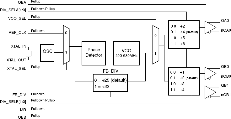
- Three LVDS outputs on two banks, Bank A with one LVDS pair and Bank B with 2 LVDS output pairs
- Using a 19.44MHz, 20MHz, or 25MHz crystal, the two output banks can be independently set for 625MHz, 622.08MHz, 312.5MHz, 250MHz, 156.25MHz, 125MHz or 100MHz
- Selectable crystal oscillator interface or LVCMOS/LVTTL single-ended input
- VCO range: 490MHz to 680MHz
- RMS phase jitter at 125MHz (1.875MHz – 20MHz): 0.50ps (typical)
- Full 3.3V output supply mode
- -40°C to 85°C ambient operating temperature
- Available in lead-free (RoHS 6) package
Description
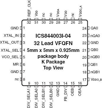
The 844003I-04 is a 3 differential output LVDS synthesizer designed to generate Ethernet reference clock frequencies. Using a 19.44MHz, 20MHz or 25MHz, 18pF parallel resonant crystal, the following frequencies can be generated based on the settings of four frequency select pins (DIV_SELA[1:0], DIV_SELB[1:0]): 625MHz, 622.08MHz, 312.5MHz, 250MHz, 156.25MHz, 125MHz and 100MHz. The 844003I-04 has two output banks, Bank A with one differential LVDS output pair and Bank B with two differential LVDS output pairs. The two banks have their own dedicated frequency select pins and can be independently set for the frequencies mentioned above. The 844003I-04 uses our third generation low phase noise VCO technology and can achieve 1ps or lower typical rms phase jitter, easily meeting Ethernet jitter requirements. The 844003I-04 is packaged in a 32-pin VFQFN package.