
Features
- Fourth generation FemtoClock™ Next Generation (NG) technology
- Three differential HCSL outputs, one differential LVPECL and two single-ended LVCMOS/LVTTL outputs
- Crystal oscillator interface designed for a 25MHz, 12pF parallel resonant crystal
- CLK/nCLK input pair can accept the following differential input levels: LVPECL, LVDS, HCSL
- A 25MHz crystal generates output frequencies of: 100MHz, 50MHz and 25MHz
- VCO frequency: 2GHz
- RMS Phase Jitter @ 100MHz, (12kHz – 20MHz) using a 25MHz crystal: 0.36ps (maximum)
- Power supply noise rejection PSNR: -45dB (typical)
- PCI Express Gen 2 (5 Gb/s) jitter compliant
- Full 3.3V supply mode
- -40°C to 85°C ambient operating temperature
- Available in lead-free (RoHS 6) package
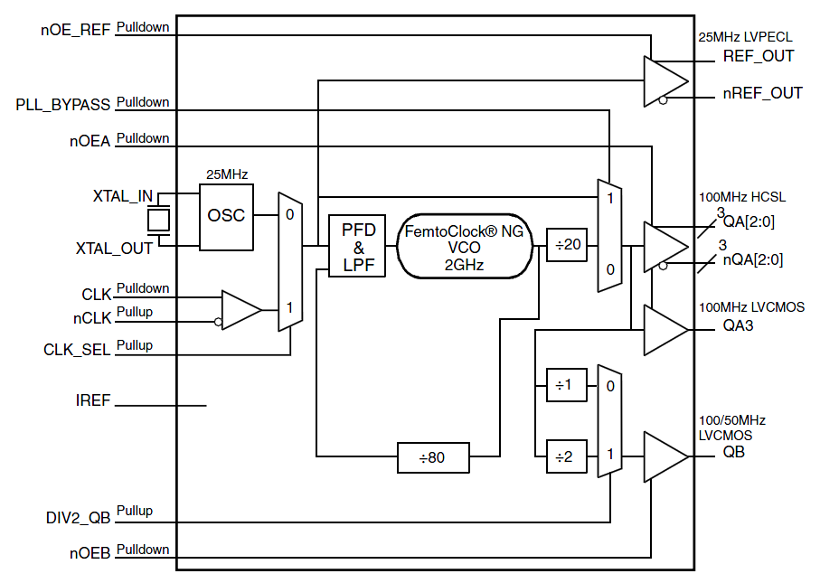
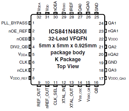
841N4830I - Block Diagram
Description
The 841N4830 is a 3 HCSL, 1 LVPECL and 2 LVCMOS output Synthesizer optimized to generate PCI Express reference clock frequencies. The device uses Renesas' fourth generation FemtoClock™ NG technology for synthesis of high clock frequency at very low phase noise. It provides low power consumption with good power supply noise rejection. Using a 25MHz, 12pF parallel resonant crystal, the following frequencies can be generated: 100MHz, 50MHz and 25MHz. Maximum rms phase jitter of 0.27ps, easily meets PCI Express jitter requirements. The 841N4830 is packaged in a small 32-pin VFQFN package.
Parameters
| Attributes | Value |
|---|---|
| Temp. Range (°C) | -40 to 85°C |
| Product Category | FemtoClock, Low Jitter Clocks (<700 fs RMS) |
Package Options
| Pkg. Type | Pkg. Dimensions (mm) | Lead Count (#) | Pitch (mm) |
|---|---|---|---|
| VFQFPN | 5.0 x 5.0 x 0.9 | 32 | 0.5 |

Support Communities
Get quick technical support online from Renesas Engineering Community technical staff.

Knowledge Base
Browse our knowledge base for helpful articles, FAQs, and other useful resources.

