
Features
- Twelve LVCMOS/LVTTL outputs
- CLK input supports the following input types: LVCMOS, LVTTL
- Maximum output frequency: 250MHz
- Output skew: 160ps (maximum)
- Supply modes:
Core/Output
3.3V/3.3V
3.3V/2.5V
3.3V/1.8V
2.5V/2.5V
2.5V/1.8V
1.8V/1.8V - -40°C to 85°C ambient operating temperature
- Available in lead-free (RoHS 6) package
Description
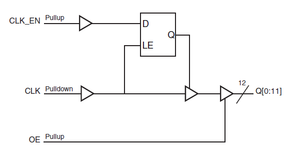
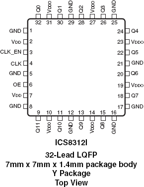
The 8312I is a low skew, 1-to-12 LVCMOS/ LVTTL Fanout Buffer and a member of the family of High Performance Clock Solutions from IDT. The 8312I single-ended clock input accepts LVCMOS or LVTTL input levels. The low impedance LVCMOS outputs are designed to drive 50Ω series or parallel terminated transmission lines. The effective fanout can be increased from 12 to 24 by utilizing the ability of the outputs to drive two series terminated lines. The 8312I is characterized at full 3.3V, 2.5V, and 1.8V, mixed 3.3V/2.5V, 3.3V/1.8V and 2.5V/1.8V output operating supply modes. Guaranteed output and part-to-part skew characteristics along with the 1.8V output capabilities makes the 8312I ideal for high performance, single ended applications that also require a limited output voltage.

Support Communities


